DESCRIPTION
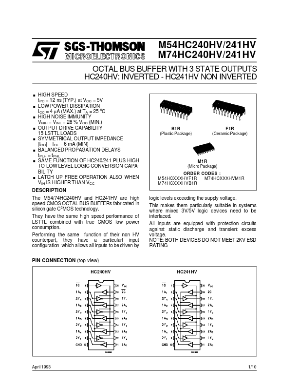
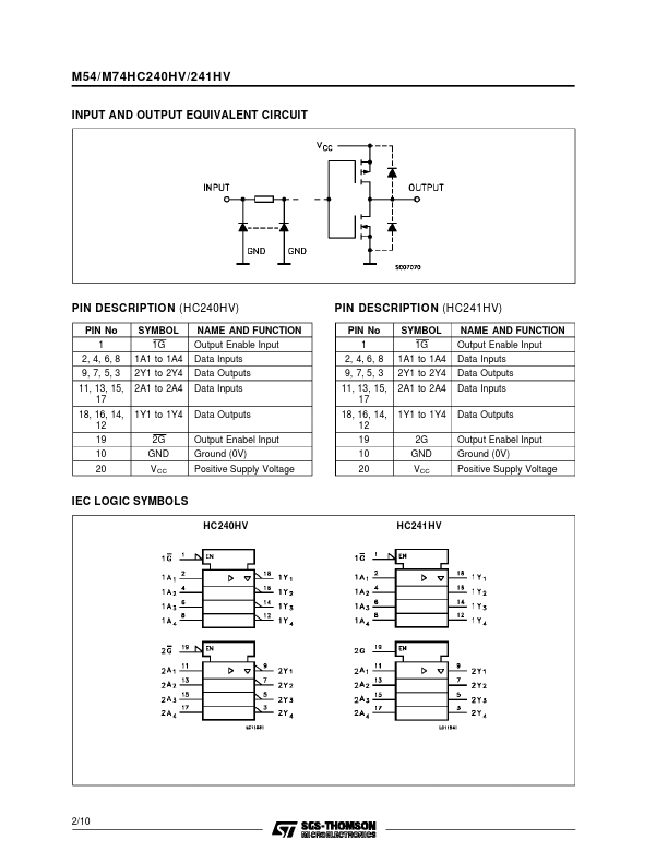
Performing the same function of their non HV counterpart, they have a particularl input configuration which allows all inputs to be driven by PIN CONNECTION (top view) HC240HV HC241HV logic levels exceeding the supply voltage. This makes them particularly suitable in systems where mixed 3V/5V logic devices need to be interfaced. All inputs are equipped with protection circuits against static discharge and transient excess voltage. NOTE: BOTH DEVICES DO NOT MEET 2KV ESD RATING April 1993 1/10 M54/M74HC240HV/241HV INPUT AND OUTPUT EQUIVALENT CIRCUIT PIN DESCRIPTION
(HC240HV) PIN No 1 2, 4, 6, 8 9, 7, 5, 3 11, 13, 15, 17 18, 16, 14, 12 19 10 20 SYMBOL 1G 1A1 to 1A4 2Y1 to 2Y4 2A1 to 2A4 1Y1 to 1Y4 2G GND V CC NAME AND FUNCTION Output Enable Input Data Inputs Data Outputs Data Inputs Data Outputs Output Enabel Input Ground (0V) Positive Supply Voltage PIN DESCRIPTION
(HC241HV) PIN No 1 2, 4, 6, 8 9, 7, 5, 3 11, 13, 15, 17 18, 16, 14, 12 19 10 20 SYMBOL 1G 1A1 to 1A4 2Y1 to 2Y4... STMicroelectronics