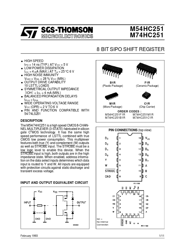
DESCRIPTION
This multiplexer features both true (Y) and complement (W) outputs as well as STROBE input. The STROBE must be a low logic level to enable this device. When the STROBE input is high, both outputs are in the high impedance state. When enabled, address information on the data select inputs determines which data input is routed to Y and W. All inputs are equipped with protection circuits against static discharge and transient excess voltage. PIN CONNECTIONS (top view) INPUT AND OUTPUT EQUIVALENT CIRCUIT NC = No Internal Connection February 1993 1/11 M54/M74HC251 TRUTH TABLE INPUTS C X L L L L H H H H X: Don’t Care Z: HIGH Impedance OUTPUS A X L H L H L H L H STROBE S H L L L L L L L L Y Z D0 D1 D2 D3 D4 D5 D6 D7 W Z D0 D1 D2 D3 D4 D5 D6 D7 B X L L H H L L H H LOGIC DIAGRAM 2/11 M54/M74HC251 PIN DESCRIPTION
PIN No 4, 3, 2, 1, 15, 14, 13, 12 5 6 7 11, 10, 9 8 16 SYMBOL D0 to D7 NAME AND FUNCTION Multiplexer Inputs IEC LOGIC SYMBOL Y W STROBE A, B, C GND V CC Multiplexer Output C... STMicroelectronics