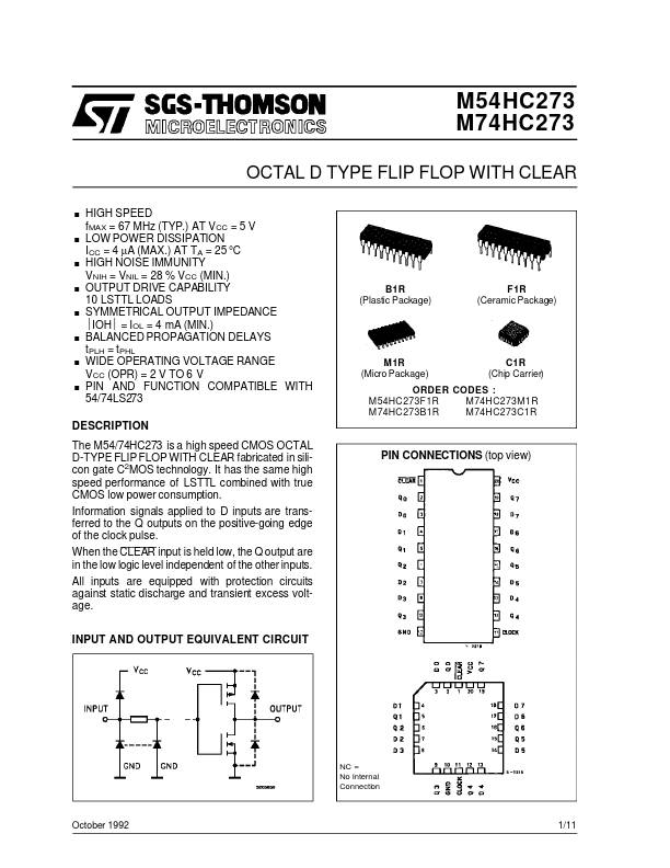
DESCRIPTION
Information signals applied to D inputs are transferred to the Q outputs on the positive-going edge of the clock pulse. When the CLEAR input is held low, the Q output are in the low logic level independent of the other inputs. All inputs are equipped with protection circuits against static discharge and transient excess voltage. INPUT AND OUTPUT EQUIVALENT CIRCUIT PIN CONNECTIONS (top view) NC = No Internal Connection October 1992 1/11 M54/M74HC273 PIN DESCRIPTION
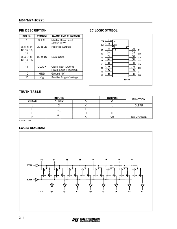
PIN No 1 2, 5, 6, 9, 12, 15, 16, 19 3, 4, 7, 8, 13, 14, 17, 18 11 10 20 SYMBOL CLEAR Q0 to Q7 NAME AND FUNCTION Master Reset Input (Active LOW) Flip Flop Outputs IEC LOGIC SYMBOL D0 to D7 Data Inputs CLOCK GND V CC Clock Input (LOW to HIGH, Edge Triggered) Ground (0V) Positive Supply Voltage TRUTH TABLE CLEAR L H H H X: Don’t Care INPUTS CLOCK X D X L H X OUTPUS Q L L H Qn FUNCTION CLEAR NO CHANGE LOGIC DIAGRAM 2/11 M54/M74HC273 ABSOLUTE MAXIMUM RATINGS
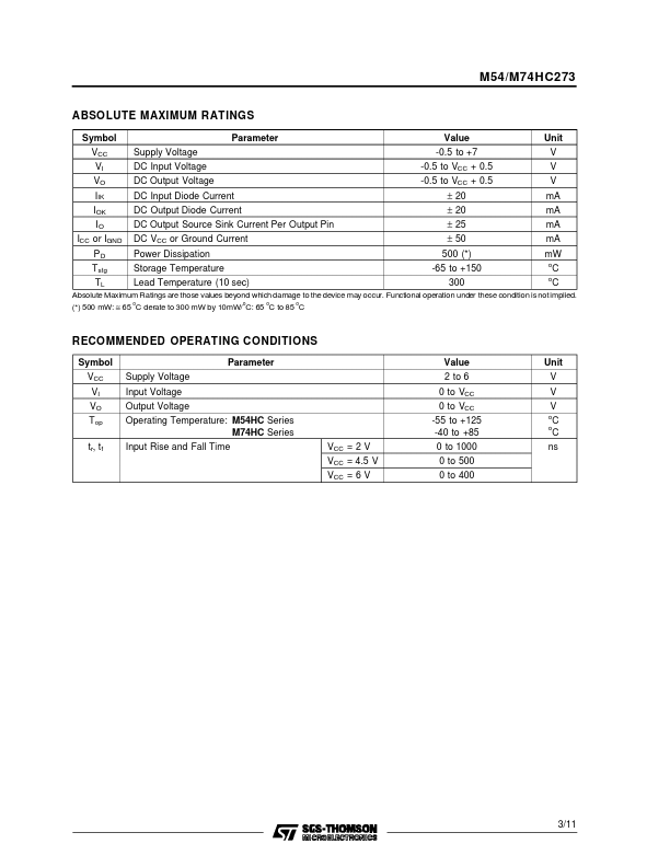
Symbol VCC VI VO IIK IOK IO ICC or IGND PD Tstg TL Supply Vol... STMicroelectronics