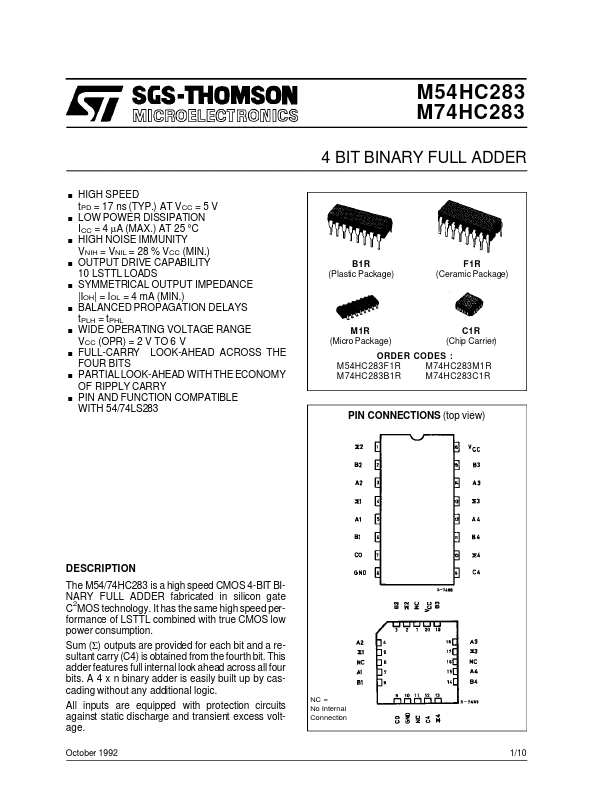
DESCRIPTION
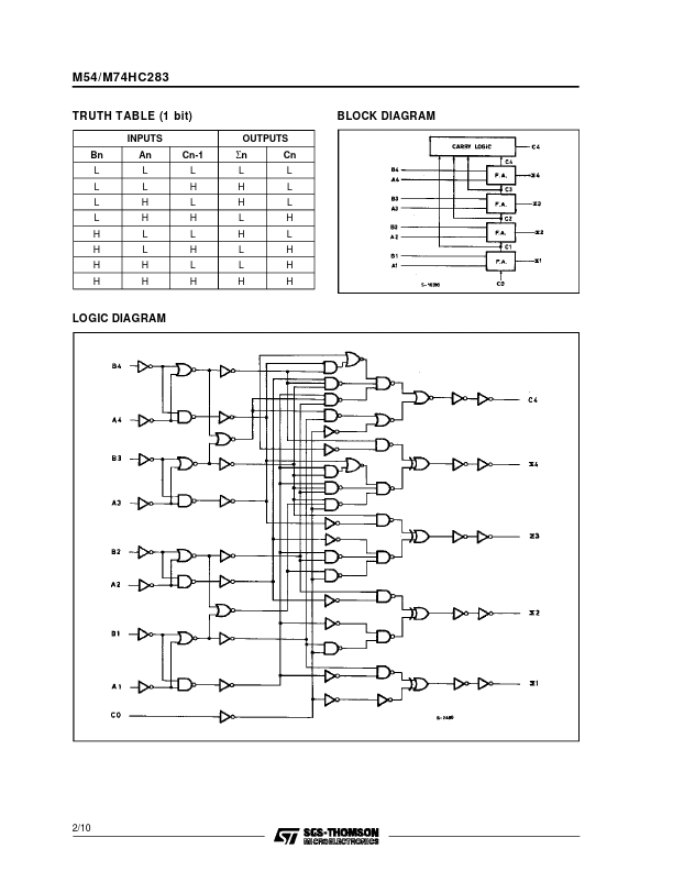
Sum (Σ) outputs are provided for each bit and a resultant carry (C4) is obtained from the fourth bit. This adder features full internal look ahead across all four bits. A 4 x n binary adder is easily built up by cascading without any additional logic. All inputs are equipped with protection circuits against static discharge and transient excess voltage. October 1992 NC = No Internal Connection 1/10 M54/M74HC283 TRUTH TABLE (1 bit) INPUTS Bn L L L L H H H H An L L H H L L H H Cn-1 L H L H L H L H OUTPUTS Σn L H H L H L L H Cn L L L H L H H H BLOCK DIAGRAM LOGIC DIAGRAM 2/10 M54/M74HC283 INPUT AND OUTPUT EQUIVALENT CIRCUIT PIN DESCRIPTION
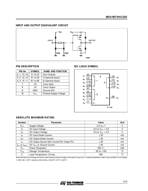
PIN No 4, 1, 13, 10 5, 3, 14, 12 6, 2, 15, 11 7 9 8 16 SYMBOL Σ1 to Σ4 A1 to A4 B1 to B4 C0 C4 GND V CC NAME AND FUNCTION Sum Outputs A Operand Inputs B Operand Inputs Carry Input Carry Output Ground (0V) Positive Supply Voltage IEC LOGIC SYMBOL ABSOLUTE MAXIMUM RATING Symbol VCC VI VO IIK IOK IO ICC or IGND PD Tstg TL Supply Voltage DC Inpu... STMicroelectronics