DESCRIPTION
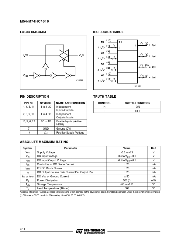
The C input is provided to control the switch ; the switch is ON when the C input is held high and off when C is held low. October 1993 NC = No Internal Connection 1/11 M54/M74HC4016 LOGIC DIAGRAM IEC LOGIC SYMBOL PIN DESCRIPTION
PIN No 1, 4, 8, 11 2, 3, 9, 10 13, 5, 6, 12 7 14 SYMBOL 1 to 4 I/O 1 to 4 O/I 1C to 4C GND VCC NAME AND FUNCTION Independent Inputs/Outputs Independent Outputs/Inputs Enable Inputs (Active HIGH) Ground (0V) Positive Supply Voltage TRUTH TABLE CONTROL H L SWITCH FUNCTION ON OFF ABSOLUTE MAXIMUM RATING Symbol VCC VIN VI/O IOK II/OK IO ICC or IGND PD Tstg TL Supply Voltage DC Input Voltage DC Input/Output Voltage Control Input DC Diode Current I/O DC Diode Current DC Output Source Sink Current Per Output Pin DC VCC or Ground Current Power Dissipation Storage Temperature Lead Temperature (10 sec) Parameter Value -0.5 to +13 -0.5 to VCC + 0.5 -0.5 to VCC + 0.5 ± 20 ± 20 ± 25 ± 50 500 (*) -65 to +150 300 Unit V V V mA mA mA mA mW o o C C ABSOLUTE MAXIMUM RATINGS
are those values beyond which damage to the device may occur. STMicroelectronics