DESCRIPTION
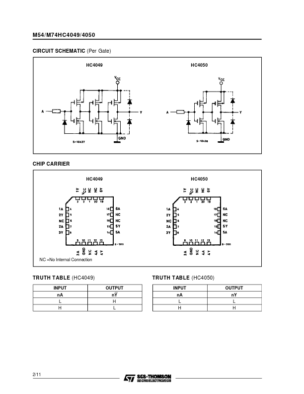
The M54/75HC4049 is an inverting buffer, while the M54/74HC4050 is a non-inverting buffer. The internal circuit is composed of 3 stage or 2stage inverters, which provides high noise immunity and a stable output. Input protection circuits are different from those of the high speed CMOS IC’s. The VCC side diodes are designed to allow logiclevel convertion from high-level voltages (up to 15 V) to low-level voltages. March 1993 NC = No Internal Connection HC4050 1/11 M54/M74HC4049/4050 CIRCUIT SCHEMATIC (Per Gate) HC4049 HC4050 CHIP CARRIER HC4049 HC4050 NC =No Internal Connection TRUTH TABLE (HC4049) INPUT nA L H OUTPUT nY H L TRUTH TABLE (HC4050) INPUT nA L H OUTPUT nY L H 2/11 M54/M74HC4049/4050 PIN DESCRIPTION
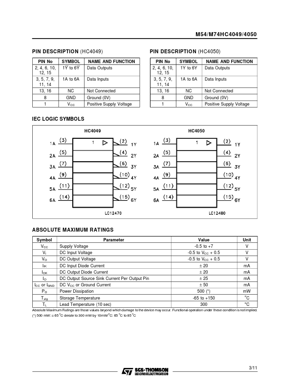
(HC4049) PIN No 2, 4, 6, 10, 12, 15 3, 5, 7, 9, 11, 14 13, 16 8 1 SYMBOL 1Y to 6Y 1A to 6A NC GND V CC NAME AND FUNCTION Data Outputs Data Inputs Not Connected Ground (0V) Positive Supply Voltage PIN DESCRIPTION
(HC4050) PIN No 2, 4, 6, 10, 12, 15 3, 5, 7, 9, 11, 14 1... STMicroelectronics