DESCRIPTION
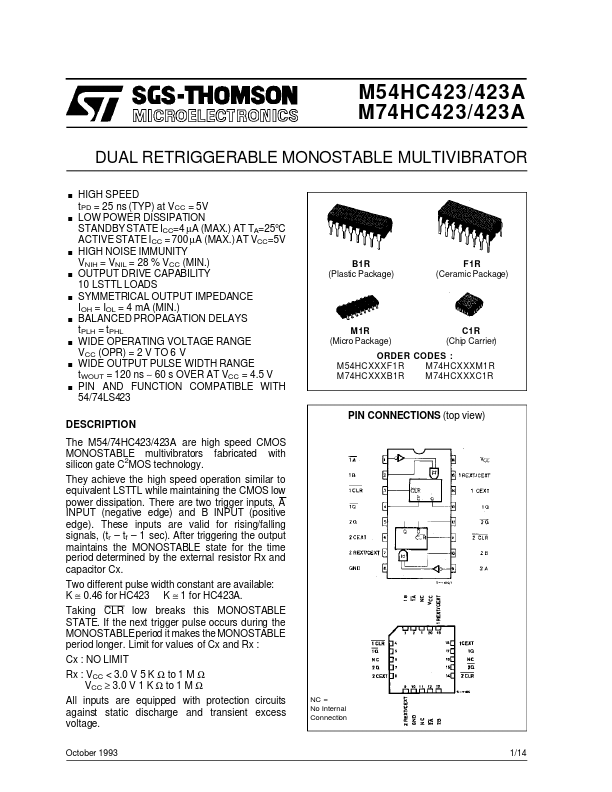
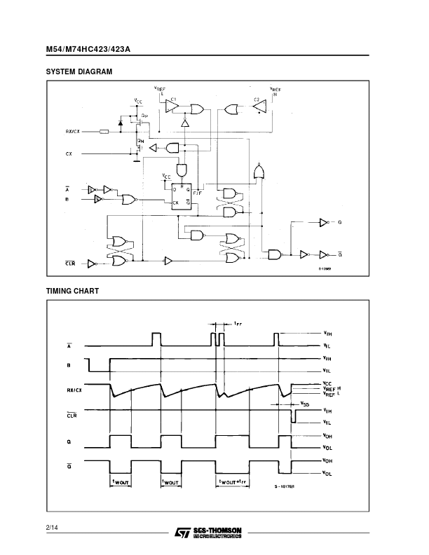
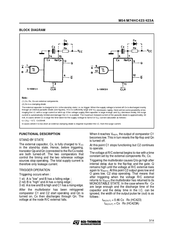
There are two trigger inputs, A INPUT (negative edge) and B INPUT (positive edge). These inputs are valid for rising/falling signals, (tr – tf – 1 sec). After triggering the output maintains the MONOSTABLE state for the time period determined by the external resistor Rx and capacitor Cx. Two different pulse width constant are available: K ≅ 0.46 for HC423 K ≅ 1 for HC423A. Taking CLR low breaks this MONOSTABLE STATE. If the next trigger pulse occurs during the MONOSTABLEperiod it makes the MONOSTABLE period longer. Limit for values of Cx and Rx : Cx : NO LIMIT Rx : VCC < 3.0 V 5 K Ω to 1 M Ω VCC ≥ 3.0 V 1 K Ω to 1 M Ω All inputs are equipped with protection circuits against static discharge and transient excess voltage. October 1993 PIN CONNECTIONS (top view) NC = No Internal Connection 1/14 M54/M74HC423/423A SYSTEM DIAGRAM TIMING CHART 2/14 M54/M74HC423/423A BLOCK DIAGRAM Note : (1) Cx, Rx, Dx are external components. (2) Dx is a clamping diode. The external capacitor is charged to VCC inthe stand-by state, i.e. no trigger. STMicroelectronics