DESCRIPTION
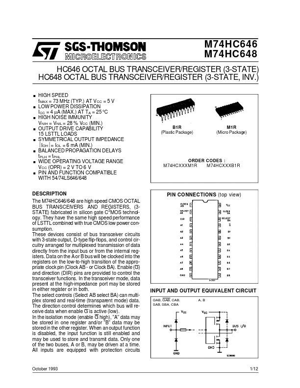
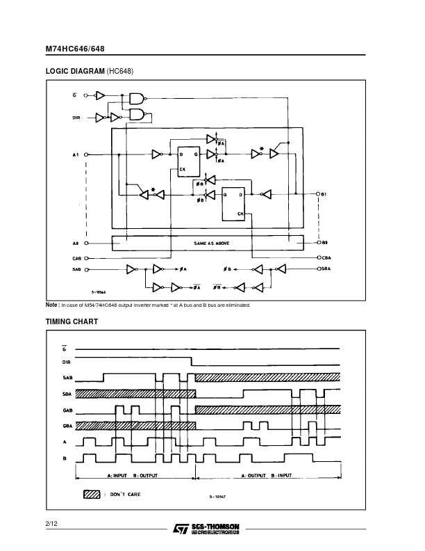
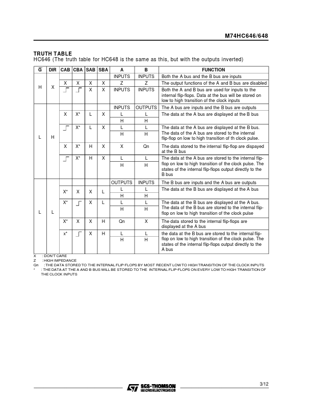
Data on the A or B bus will be clocked into the registers on the low-to-high transition of the appropriate clock pin (Clock AB - or Clock BA). Enable (G) and direction (DIR) pins are provided to control the transceiver functions. In the transceiver mode, data present at the high-impedance port may be stored in either register or in both. The select controls (Select AB select BA) can multiplex stored and real-time (transparent mode) data. The direction control determines which bus will receive data when enable G is active (low). In the isolation mode (enable G high), ”A” data may be stored in one register and/or ”B” data may be stored in the other register. When an output function is disabled, the input function is still enabled and may be used to store and transmit data. Only one of the two buses, A or B, may be driven at a time. All inputs are equipped with protection circuits PIN CONNECTIONS (top view) INPUT AND OUTPUT EQUIVALENT CIRCUIT GAB, GAB, CAB, SAB, SBA, CBA A, B October 1993 1/12 M74HC646/648 LOGIC DIAGRAM (HC648) Note : In case of M54/74HC646 output inverter marked * at A bus and B bus are eliminated. STMicroelectronics