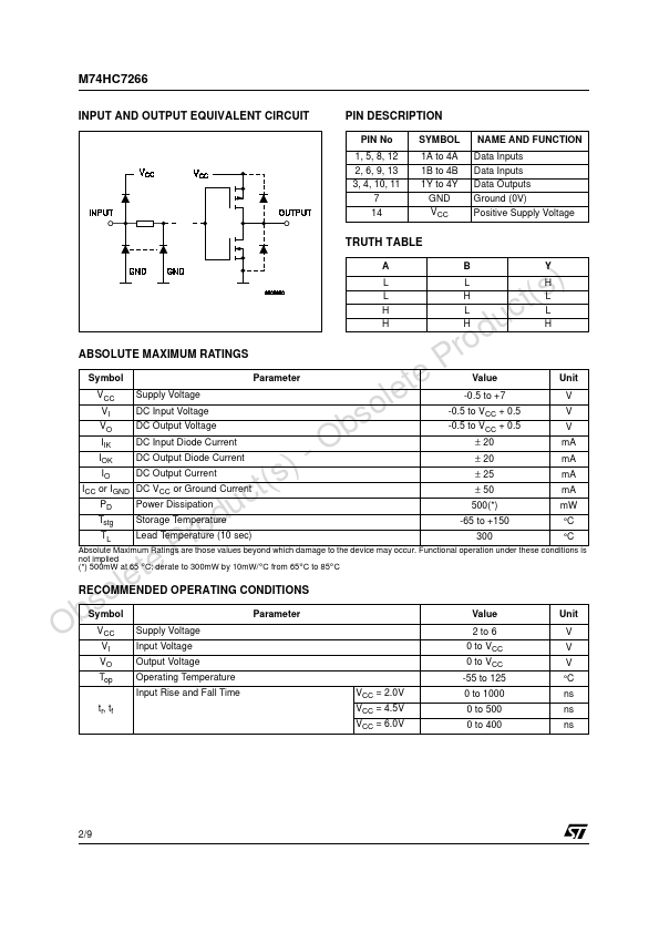
DESCRIPTION
PIN No 1, 5, 8, 12 2, 6, 9, 13 3, 4, 10, 11 7 14 SYMBOL 1A to 4A 1B to 4B 1Y to 4Y GND VCC NAME AND FUNCTION Data Inputs Data Inputs Data Outputs Ground (0V) Positive Supply Voltage TRUTH TABLE ABY )L L H t(sL H L HLL ucH H H rodABSOLUTE MAXIMUM RATINGS
PSymbol Parameter Value Unit leteVCC Supply Voltage -0.5 to +7 V oVI DC Input Voltage -0.5 to VCC + 0.5 V sVO DC Output Voltage -0.5 to VCC + 0.5 V bIIK DC Input Diode Current ± 20 mA - OIOK DC Output Diode Current ± 20 mA )IO DC Output Current ± 25 mA t(sICC or IGND DC VCC or Ground Current ± 50 mA cPD Power Dissipation 500(*) mW duTstg Storage Temperature -65 to +150 °C roTL Lead Temperature (10 sec) 300 °C ABSOLUTE MAXIMUM RATINGS
are those values beyond which damage to the device may occur. Functional operation under these conditions is Pnot implied te(*) 500mW at 65 °C; derate to 300mW by 10mW/°C from 65°C to 85°C leRECOMMENDED OPERATING CONDITIONS soSymbol Ob VCC Supply Voltage Parameter Value 2 to 6 Unit V VI Input Voltage 0 to VCC V VO Output Voltage 0 to VCC V Top Operating Temperature -55 to 125 °C Input Rise and Fall Time VCC = 2.0V 0 to 1000 ns tr, tf VCC = 4. STMicroelectronics