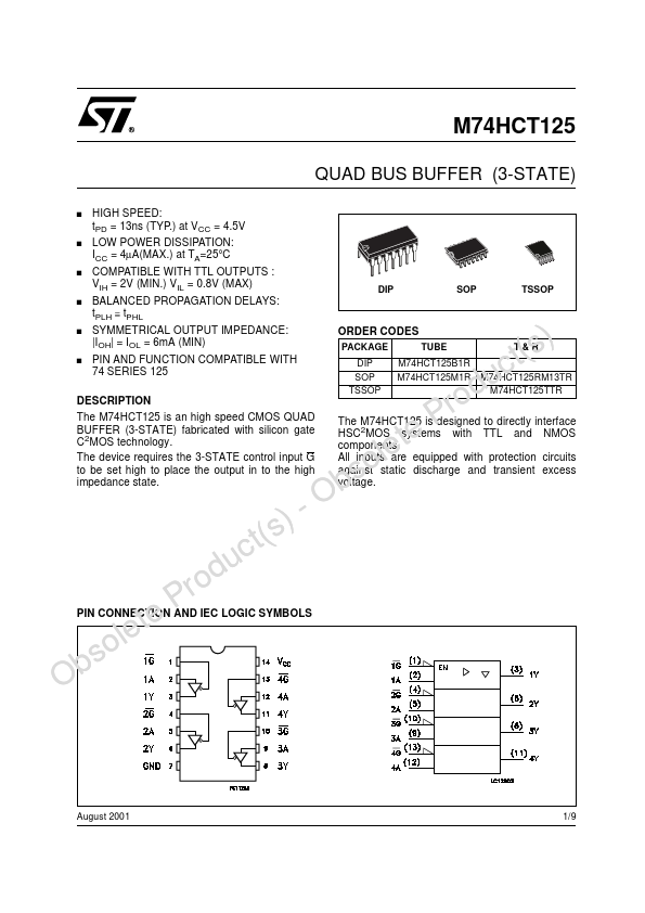
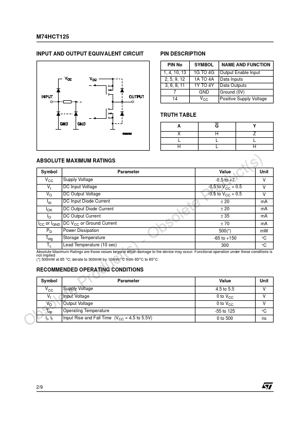
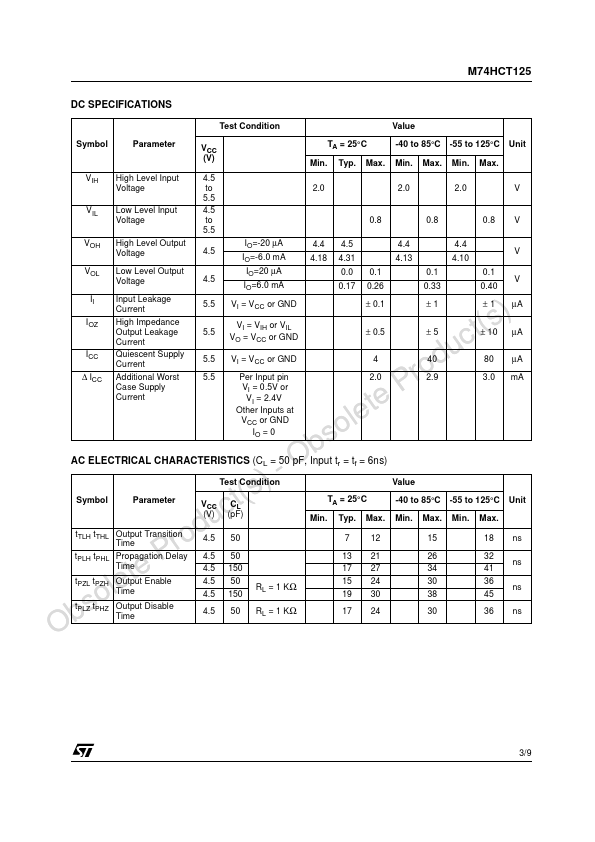
DESCRIPTION
PIN No 1, 4, 10, 13 2, 5, 9, 12 3, 6, 8, 11 7 14 SYMBOL 1G TO 4G 1A TO 4A 1Y TO 4Y GND VCC NAME AND FUNCTION Output Enable Input Data Inputs Data Outputs Ground (0V) Positive Supply Voltage TRUTH TABLE AGY XHZ LLL HLH ABSOLUTE MAXIMUM RATINGS
t(s)Symbol Parameter Value Unit cVCC Supply Voltage -0.5 to +7 V duVI DC Input Voltage -0.5 to VCC + 0.5 V roVO DC Output Voltage -0.5 to VCC + 0.5 V PIIK DC Input Diode Current ± 20 mA teIOK DC Output Diode Current ± 20 mA leIO DC Output Current ± 35 mA oICC or IGND DC VCC or Ground Current ± 70 mA bsPD Power Dissipation 500(*) mW OTstg Storage Temperature -65 to +150 °C -TL Lead Temperature (10 sec) 300 °C )ABSOLUTE MAXIMUM RATINGS
are those values beyond which damage to the device may occur. Functional operation under these conditions is t(snot implied (*) 500mW at 65 °C; derate to 300mW by 10mW/°C from 65°C to 85°C ucRECOMMENDED OPERATING CONDITIONS rodSymbol PVCC teVI leVO oTop Obstr, tf Parameter Supply Voltage Input Voltage Outp... STMicroelectronics