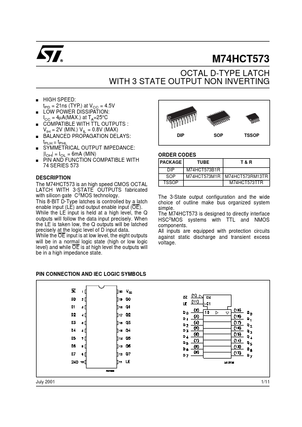
DESCRIPTION
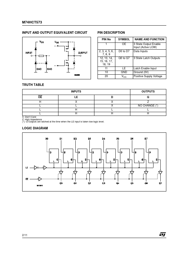
While the LE input is held at a high level, the Q outputs will follow the data input precisely. While the OE input is at low level, the eight outputs will be in a normal logic state (high or low logic level) and while OE is at high level the outputs will be in a high impedance state. The 3-State output configuration and the wide choice of outline make bus organized system simple. The M74HCT573 is designed to directly interface HSC2MOS systems with TTL and NMOS components. All inputs are equipped with protection circuits against static discharge and transient excess voltage. PIN CONNECTION AND IEC LOGIC SYMBOLS July 2001 1/11 M74HCT573 INPUT AND OUTPUT EQUIVALENT CIRCUIT PIN DESCRIPTION
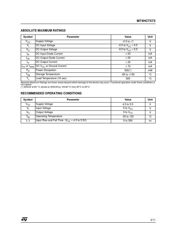
PIN No 1 2, 3, 4, 5, 6, 7, 8, 9 12, 13, 14, 15, 16, 17, 18, 19 11 10 20 SYMBOL OE D0 to D7 Q0 to Q7 NAME AND FUNCTION 3 State Output Enable Input (Active LOW) Data Inputs 3 State Latch Outputs LE GND VCC Latch Enable Input Ground (0V) Positive Supply Voltage TRUTH TABLE INPUTS OE H L L L LE X... STMicroelectronics