DESCRIPTION
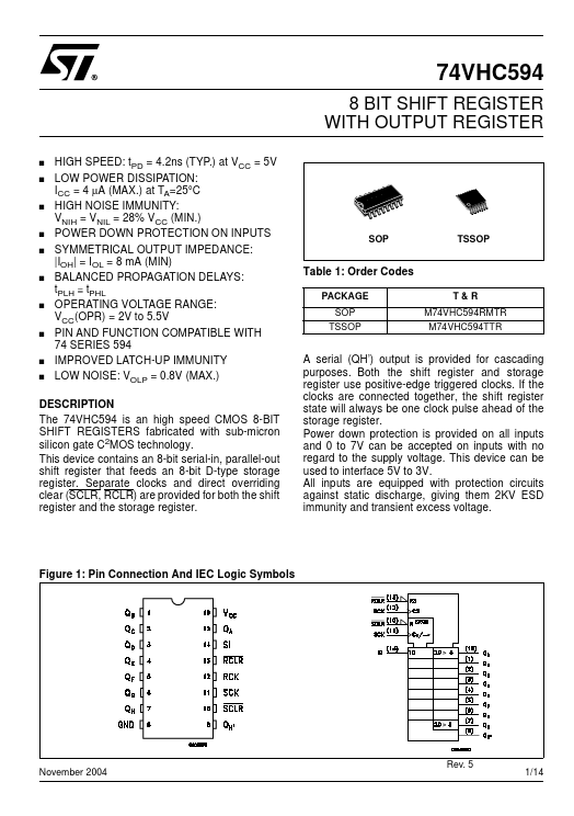
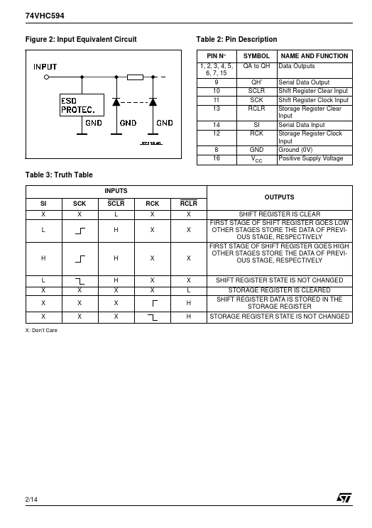
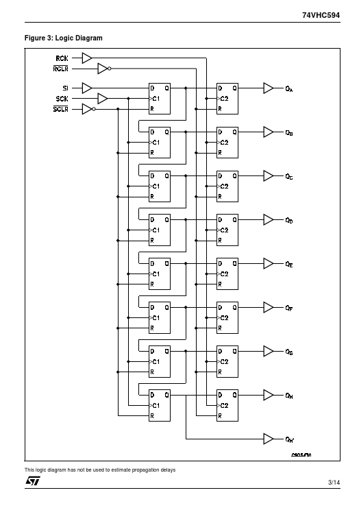
Separate clocks and direct overriding clear (SCLR, RCLR) are provided for both the shift register and the storage register. A serial (QH’) output is provided for cascading purposes. Both the shift register and storage register use positive-edge triggered clocks. If the clocks are connected together, the shift register state will always be one clock pulse ahead of the storage register. Power down protection is provided on all inputs and 0 to 7V can be accepted on inputs with no regard to the supply voltage. This device can be used to interface 5V to 3V. All inputs are equipped with protection circuits against static discharge, giving them 2KV ESD immunity and transient excess voltage. Figure 1: Pin Connection And IEC Logic Symbols November 2004 Rev. 5 1/14 74VHC594 Figure 2: Input Equivalent Circuit Table 2: Pin DESCRIPTION
PIN N° 1, 2, 3, 4, 5, 6, 7, 15 9 10 11 13 14 12 8 16 SYMBOL QA to QH QH’ SCLR SCK RCLR SI RCK GND VCC NAME AND FUNCTION Data Outputs Serial Data Output S... STMicroelectronics