STMicroelectronics NAND04GW3C2A
Multi-level NAND Flash Memory
| Part No. | NAND04GW3C2A |
|---|---|
| Datasheet | NAND04GW3C2A Download |
| Manufacturer |  STMicroelectronics |
| Description | Multi-level NAND Flash Memory |
| Buy | Stock & Price |
FEATURES
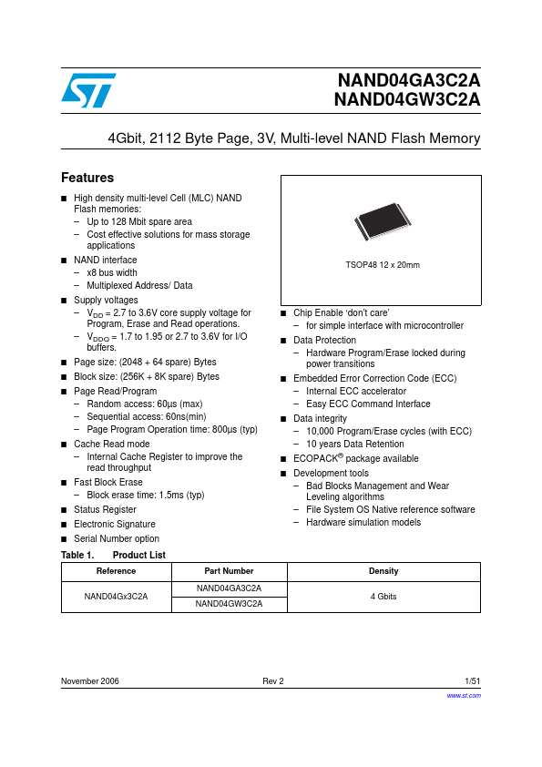
● High density multi-level Cell (MLC) NAND Flash memories: – Up to 128 Mbit spare area – Cost effective solutions for mass storage applications NAND interface – x8 bus width – Multiplexed Address/ Data Supply voltages – VDD = 2.7 to 3.6V core supply voltage for Program, Erase and Read operations. – VDDQ = 1.7 to 1.95 or 2.7 to 3.6V for I/O buffers. Page size: (2048 + 64 spare) Bytes Block size: (256K + 8K spare) Bytes Page Read/Program – Random access: 60µs (max) – Sequential access: 60ns(min) – Page Program Operation time: 800µs (typ) Cache Read mode – Internal Cache Register to improve the read throughput Fast Block Erase – Block erase time: 1.5ms (typ) Status Register Electronic Signature Serial Number option Product List Reference NAND04Gx3C2A NAND04GW3C2A Part Number NAND04GA3C2A 4 Gbits Density●
●
● TSOP48 12 x 20mm
● Chip Enable ‘don’t care’ – for simple interface with microcontroller Data Protection – Hardware Program/Erase locked during power transitions Embedded Err...