Datasheet4U Logo Datasheet4U.com

P25NM60N - N-CHANNEL MOSFET

Datasheet Summary

Description

The STP25NM60N is realized with the second generation of MDmesh Technology.

This revolutionary MOSFET associates a new vertical structure to the Company's strip layout to yield the world's lowest on-resistance and gate charge.

Features

  • TYPE STB25NM60N-1 STF25NM60N STP25NM60N STW25NM60N STB25NM60N s s s s s STP25NM60N - STF25NM60N STB25NM60N/-1 - STW25NM60N.

📥 Download Datasheet

Datasheet preview – P25NM60N

Datasheet Details

Part number P25NM60N
Manufacturer STMicroelectronics
File Size 572.40 KB
Description N-CHANNEL MOSFET
Datasheet download datasheet P25NM60N Datasheet
Additional preview pages of the P25NM60N datasheet.
Other Datasheets by STMicroelectronics

Full PDF Text Transcription

Click to expand full text
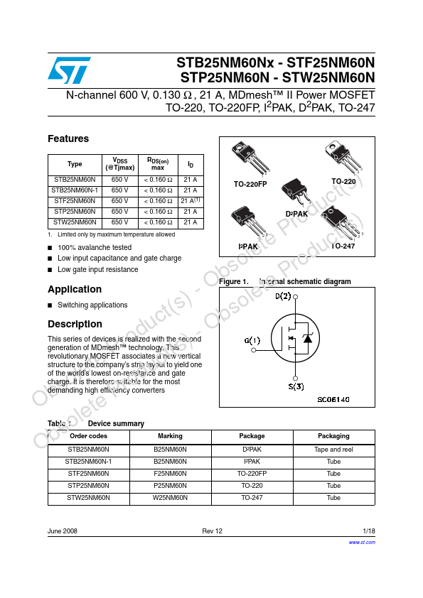
N-CHANNEL 600V 0.140Ω-20A TO-220/FP/D²/I²PAK/TO-247 SECOND GENERATION MDmesh™ MOSFET Table 1: General Features TYPE STB25NM60N-1 STF25NM60N STP25NM60N STW25NM60N STB25NM60N s s s s s STP25NM60N - STF25NM60N STB25NM60N/-1 - STW25NM60N PRODUCT PREVIEW Figure 1: Package RDS(on) < 0.170 Ω < 0.170 Ω < 0.170 Ω < 0.170 Ω < 0.170 Ω ID 20 A 20(*) A 20 A 20 A 20 A VDSS (@Tjmax) 650 V 650 V 650 V 650 V 650 V 3 1 2 1 3 2 TO-220 3 1 TO-220FP s WORLD’S LOWEST ON RESISTANCE TYPICAL RDS(on) = 0.140 Ω HIGH dv/dt AND AVALANCHE CAPABILITIES 100% AVALANCHE TESTED LOW INPUT CAPACITANCE AND GATE CHARGE LOW GATE INPUT RESISTANCE D²PAK 3 12 3 I²PAK TO-247 Figure 2: Internal Schematic Diagram 2 1 DESCRIPTION The STP25NM60N is realized with the second generation of MDmesh Technology.
Published: |