PSD913F2
PSD913F2 is ISP Peripherals manufactured by STMicroelectronics.
FEATURES
SUMMARY s Single Supply Voltage:
- 5 V±10% for PSD9xx F2
- 3.3 V±10% for PSD9xx F2-V s Up to 2Mbit of Primary Flash Memory (8 uniform sectors) s 256Kbit Secondary Flash Memory (4 uniform sectors) s Up to 256Kbit SRAM s Over 2,000 Gates of PLD: DPLD s 27 Reconfigurable I/O ports s Enhanced JTAG Serial Port s Programmable power management s High Endurance:
- 100,000 Erase/Write Cycles of Flash Memory
- 1,000 Erase/Write Cycles of PLD
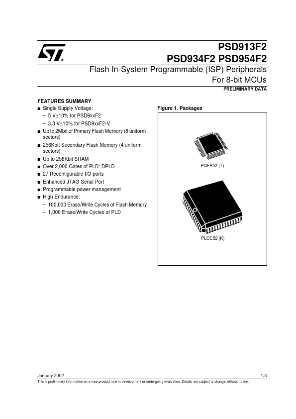
Figure 1. Packages
PQFP52 (T)
PLCC52 (K)
January 2002
1/3
This is preliminary information on a new product now in development or undergoing evaluation. Details are subject to change without notice.
PSD9XX Family
PSD913F2 PSD934F2 PSD954F2 Configurable Memory System on a Chip for 8-Bit Microcontrollers
Table of Contents
Introduction 1 In-System Programming (ISP) JTAG 2 In-Application Programming (IAP) 2
Key Features
3 Block Diagram 4 PSD9XX Family 5 Architectural Overview
Memory...