SMA428ATR
SMA428ATR is High Gain/ Low Noise Amplifier manufactured by STMicroelectronics.
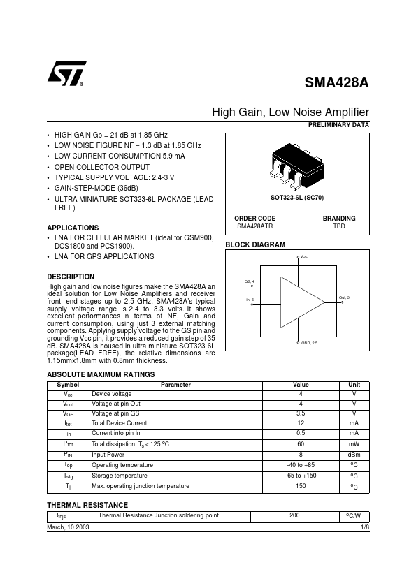
DESCRIPTION
High gain and low noise figures make the SMA428A an ideal solution for Low Noise Amplifiers and receiver front end stages up to 2.5 GHz. SMA428A’s typical supply voltage range is 2.4 to 3.3 volts. It shows excellent performances in terms of NF, Gain and current consumption, using just 3 external matching ponents. Applying supply voltage to the GS pin and grounding Vcc pin, it provides a reduced gain step of 35 d B. SMA428A is housed in ultra miniature SOT323-6L package(LEAD FREE), the relative dimensions are 1.15mmx1.8mm with 0.8mm thickness. ABSOLUTE MAXIMUM RATINGS
Symbol Vcc Vout VGS Itot Iin Ptot PIN Top Tstg Tj Device voltage Voltage at pin Out Voltage at pin GS Total Device Current Current into pin In Total dissipation, Ts < 125 o C Input Power Operating temperature Storage temperature Max. operating junction temperature Parameter Value 4 4 3.5 12 0.5 60 8 -40 to +85 -65 to +150 150 Unit V V V m A m A m W d Bm o C o C o C
SOT323-6L (SC70)
ORDER CODE SMA428ATR
BRANDING TBD
BLOCK DIAGRAM
Vcc, 1
GS, 4
In, 6
Out, 3
GND, 2;5
THERMAL RESISTANCE
Rthjs March, 10 2003 Thermal Resistance Junction soldering point 200 o C/W
1/8
SMA428A
Test Circuit (Fig. 1)
Typical application circuit (Fig. 2)
47 p F VCTRL
180 p F Supply
3 kΩ
Vcc 6.8 n H 0.5 p F RF Out
RF in
100 p F
In
Out
SMA428A
2/8
SMA428A
ELECTRICAL CHARACTERISTICS (Ta = +25o C, VCC = 2.7V, tested in circuit shown in fig.1, unless otherwise specified)
Symbol f Itot Gp NF P-1d B IIP3 LGS ICTR Parameters Frequency Range Total device current Power Gain Noise Figure (Zs = 50 Ω) Input Power at 1 d B Gain pression Input third order intercept point Insertion Loss in Gain-Step-Mode Current consumption in Gain-Step-Mode Vcc = 0.0 V, VCTRL = 2.7 V, RCTRL = 3 kΩ Vcc = 0.0 V, VCTRL = 2.7 V, RCTRL = 3 kΩ -23 -13 11 0.33 18 18 Test Conditions Min Typ 1850 5.9 21 1.3 1.7 7.5 Max Unit MHz m A d B d B d Bm d Bm d B m A
PIN CONNECTION
(Top View) 1 2 3 6 5 4
(Bottom View) 6 5 4 1 2 3
Pin No. 1 2 3 4 5 6
Pin Name...