DESCRIPTION
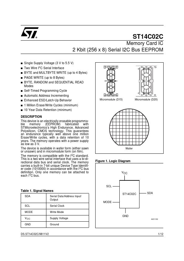
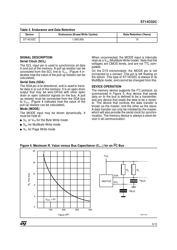
The memory operates with a power supply as low as 3 V. The device is available in wafer form (either sawn or unsawn) and in micromodule form (on film). The memory is compatible with the I2C standard. This is a two wire serial interface that uses a bi-directional data bus and serial clock. The memory carries a built-in 7-bit unique Device Type Identifier code (1010000) in accordance with the I 2C bus definition. Only one memory can be attached to each I2C bus. Wafer Figure 1. Logic Diagram VCC SCL Table 1. Signal Names SDA Serial Data/Address Input/ Output Serial Clock Write Mode Supply Voltage Ground ST14C02C MODE SDA SCL MODE VCC GND GND AI01162 DS.ST14C02C/9811V2 1/12 ST14C02C Figure 2. D15 Contact Connections Figure 3. D20 Contact Connections VCC VCC GND GND SCL SCL SDA SDA MODE AI02492 AI02491 The memory behaves as a slave device in the I2C protocol, with all memory operations synchronized by the serial clock. Read and write operations are initiated by a START condition, generated by the bus master. STMicroelectronics