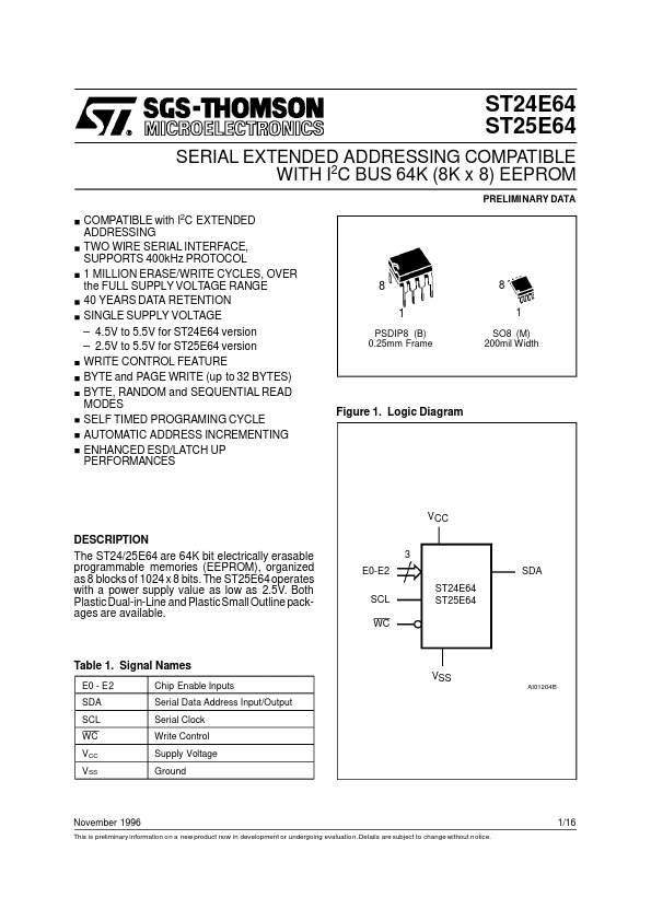
DESCRIPTION
3 E0-E2 SCL WC ST24E64 ST25E64 SDA Table 1. Signal Names E0 - E2 SDA SCL WC VCC VSS Chip Enable Inputs Serial Data Address Input/Output Serial Clock Write Control Supply Voltage Ground VSS AI01204B November 1996 This is preliminary information on a new product now in development or undergoing evaluatio n.Details are subject to change without notice. 1/16 ST24E64, ST25E64 Figure 2A. DIP Pin Connections Figure 2B. SO Pin Connections ST24E64 ST25E64 E0 E1 E2 VSS 1 2 3 4 8 7 6 5 AI01205B ST24E64 ST25E64 VCC WC SCL SDA E0 E1 E2 VSS 1 2 3 4 8 7 6 5 AI01206C VCC WC SCL SDA Table 2. ABSOLUTE MAXIMUM RATINGS
(1) Symbol TA TSTG TLEAD VIO VCC VESD Parameter Ambient Operating Temperature Storage Temperature Lead Temperature, Soldering Input or Output Voltages Supply Voltage Electrostatic Discharge Voltage (Human Body model) Electrostatic Discharge Voltage (Machine model) (3) (2) Value –40 to 125 –65 to 150 Unit °C °C °C V V V V (SO8) (PSDIP8) 40 sec 10 sec 215 260 –0.6 to 6.5 –0.3 to 6.5 4000 500 Notes: 1. STMicroelectronics