DESCRIPTION
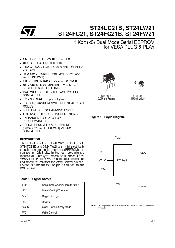
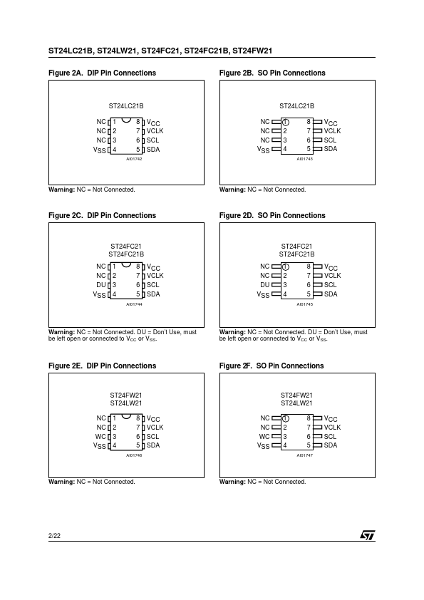
In the text, products are referred as ST24xy21, where "x" is either "L" for VESA 1 or "F" for VESA 2 compatible memories and where "y" indicates the Write Control pin connection: "C" means WC on pin 7 and "W" means WC on pin 3. 8 1 PSDIP8 (B) 0.25mm Frame 8 1 SO8 (M) 150mil Width Figure 1. Logic Diagram VCC SCL VCLK WC ST24xy21 SDA Table 1. Signal Names SDA SCL VCC VSS VCLK WC Serial Data Address Input/Output 2 Serial Clock (I C mode) VSS AI01741 Supply Voltage Ground Clock Transmit only mode Write Control Note: WC signal is only available for ST24LW21 and ST24FW21 products. June 2002 1/22 ST24LC21B, ST24LW21, ST24FC21, ST24FC21B, ST24FW21 Figure 2A. DIP Pin Connections Figure 2B. SO Pin Connections ST24LC21B NC NC NC VSS 1 2 3 4 8 7 6 5 AI01742 ST24LC21B VCC VCLK SCL SDA NC NC NC VSS 1 2 3 4 8 7 6 5 AI01743 VCC VCLK SCL SDA Warning: NC = Not Connected. Warning: NC = Not Connected. Figure 2C. DIP Pin Connections Figure 2D. SO Pin Connections ST24FC21 ST24FC21B NC NC DU VSS 1 2 3 4 8 7 6 5 AI01744 ST24FC21 ST24FC21B VCC VCLK SCL SDA NC NC DU VSS 1 2 3 4 8 7 6 5 AI01745 VCC VCLK SCL SDA Warning: NC = Not Connected. STMicroelectronics