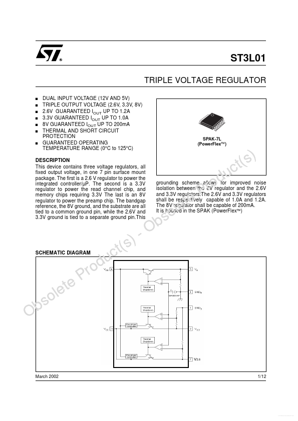
DESCRIPTION
The second is a 3.3V regulator to power the read channel chip, and memory chips requiring 3.3V The last is an 8V regulator to power the preamp chip. The bandgap reference, the 8V ground, and the substrate are all tied to a common ground pin, while the 2.6V and 3.3V ground is tied to a separate ground pin.This SCHEMATIC DIAGRAM s b O t e l o r P e u d o ) s ( ct o s b O - grounding scheme allows for improved noise isolation between the 8V regulator and the 2.6V and 3.3V regulators.The 2.6V and 3.3V regulators shall be respectively capable of 1.0A and 1.2A. The 8V regulator shall be capable of 200mA. It is housed in the SPAK (PowerFlex™) e t le o r P c u d ) s t( V2.6 March 2002 1/12 Free Datasheet ST3L01 ABSOLUTE MAXIMUM RATINGS
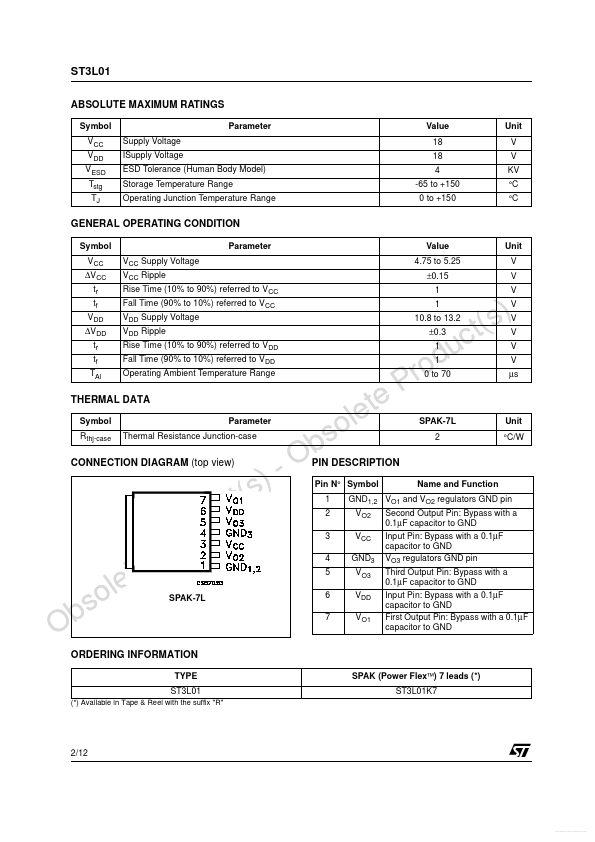
Symbol VCC VDD VESD Tstg TJ Supply Voltage ISupply Voltage ESD Tolerance (Human Body Model) Storage Temperature Range Operating Junction Temperature Range Parameter Value 18 18 4 -65 to +150 0 to +150 Unit V V KV °C °C GENERAL OPERATING CONDITION Sym... STMicroelectronics