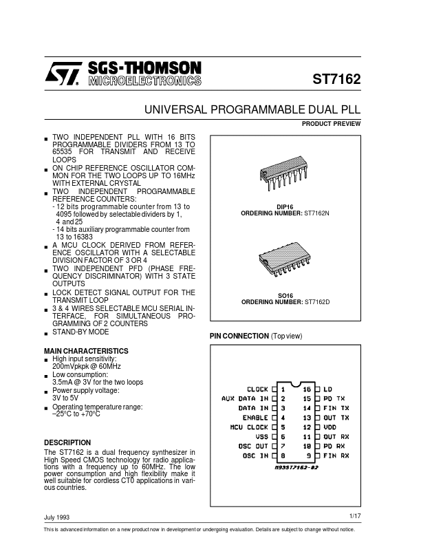
DESCRIPTION
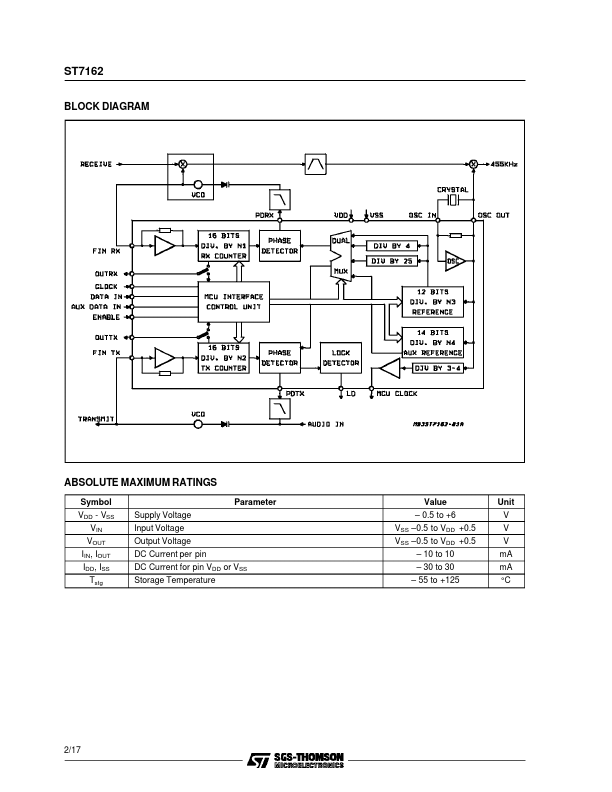
July 1993 1/17 This is advanced information on a new product now in development or undergoing evaluation. Details are subject to change without notice. ST7162 BLOCK DIAGRAM ABSOLUTE MAXIMUM RATINGS
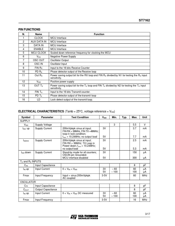
Symbol VDD - VSS VIN VOUT IIN, IOUT IDD, ISS Tstg Supply Voltage Input Voltage Output Voltage DC Current per pin DC Current for pin VDD or VSS Storage Temperature Parameter Value – 0.5 to +6 VSS –0.5 to VDD +0.5 VSS –0.5 to VDD +0.5 – 10 to 10 – 30 to 30 – 55 to +125 Unit V V V mA mA °C 2/17 ST7162 PIN FUNCTIONS N. 1 2 3 4 5 6 7 8 9 10 11 12 13 14 15 16 Name CLOCK AUX DATA IN DATA IN ENABLE MCU CLOCK VSS OSC OUT OSC IN FIN RX PD RX Out RX VDD OUT TX FIN TX PD TX LD MCU Interface MCU Interface MCU Interface MCU Interface Scaled down reference frequency for clocking the MCU Negative Power Supply Oscillator Output Oscillator Input Input to the 16 bits Receive Counter Phase detector output of the Receive loop Power saving output bit for the RX loop and FIN RX divided by N1 for testing the RX input sensitivity. STMicroelectronics