DESCRIPTION
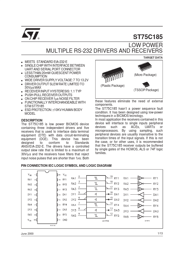
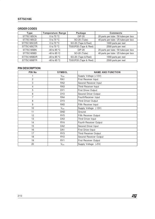
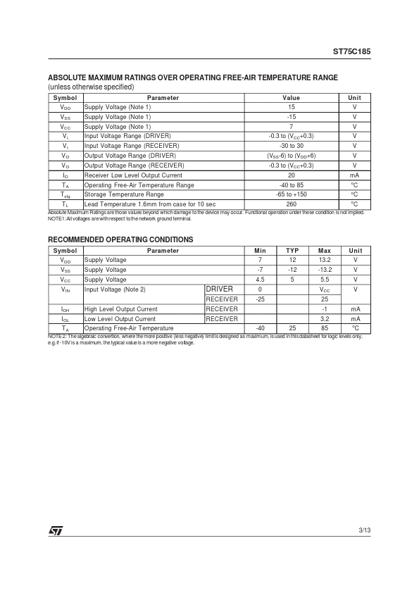
Both these features eliminate the need of external components. The ST75C185 hasn’t a power sequence fault condition. It has been designed using low-power techniques in a BICMOS tecnology. In most application the receivers contained in this device will interface to single inputs peripheral devices such as ACEs, UARTs or microprocessors. By using sampling, such peripheral devices are usuallly insensitive to the transition times of the input signals. If this is not the case, or for other uses, it is recommended that the ST75C185 receiver outputs be buffered by single gates of the HCMOS, ALS or 74F logic families. PIN CONNECTION IEC LOGIC SYMBOL AND LOGIC DIAGRAM June 2000 1/13 ST75C185 ORDER CODES T ype ST75C185CN ST75C185CD ST75C185CDR ST75C185CTR ST75C185BN ST75C185BD ST75C185BDR ST75C185BTR T emperature Ran ge 0 to 70 oC 0 to 70 oC 0 to 70 C 0 to 70 oC -40 to 85 oC -40 to 85 oC -40 to 85 oC -40 to 85 oC o Package DIP-20 SO-20 (Tube) SO-20 (Tape & Reel) TSSOP20 (Tape & Reel)... STMicroelectronics