DESCRIPTION
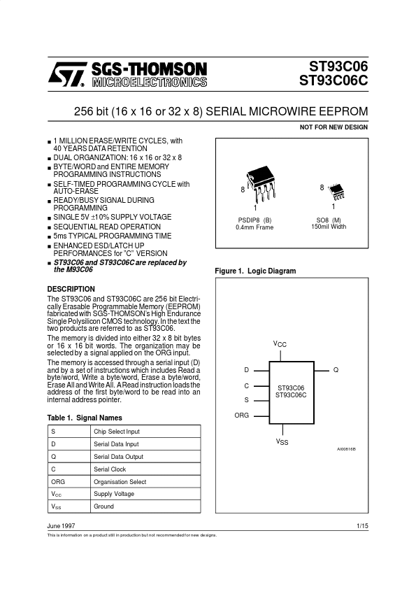
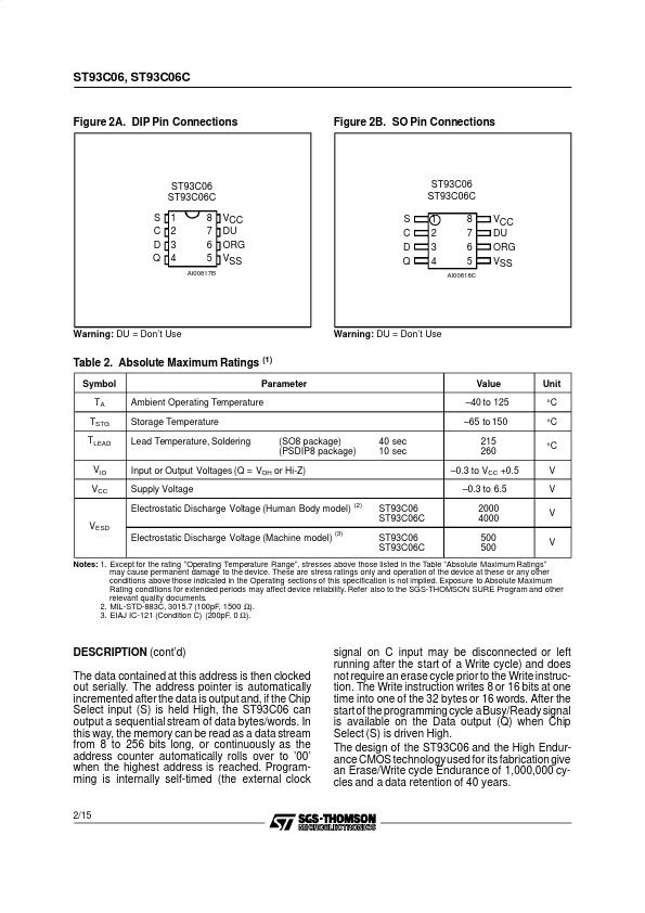
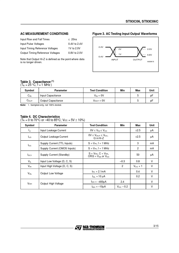
In the text the two products are referred to as ST93C06. The memory is accessed through a serial input (D) and by a set of instructions which includes Read a byte/word, Write a byte/word, Erase a byte/word, Erase All and Write All. ARead instruction loads the address of the first byte/word to be read into an internal address pointer. Table 1. Signal Names S D Q C ORG VCC VSS June 1997 Chip Select Input Serial Data Input Serial Data Output Serial Clock Organisation Select Supply Voltage Ground 8 1 PSDIP8 (B) 0.4mm Frame 8 1 SO8 (M) 150mil Width Figure 1. Logic Diagram VCC D C S ORG ST93C06 ST93C06C Q VSS AI00816B 1/15 This is information on a product still in production bu t not recommended for new de signs. ST93C06, ST93C06C Figure 2A. DIP Pin Connections Figure 2B. SO Pin Connections ST93C06 ST93C06C S C D Q 1 2 3 4 8 7 6 5 AI00817B ST93C06 ST93C06C VCC DU ORG VSS S C D Q 1 2 3 4 8 7 6 5 AI00818C VCC DU ORG VSS Warning: DU = Don’t Use Warning: DU = Don’t Use Table 2. Absol... STMicroelectronics