STMicroelectronics ST93CS66
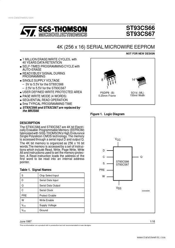
the ST93CS66 – 2.5V to 5.5V for the ST93CS67 USER DEFINED WRITE PROTECTED AREA PAGE WRITE MODE (4 WORDS) SEQUENTIAL READ OPERATION 5ms TYPICAL PROGRAMMING TIME ST93CS66 and ST93CS67 are replaced by the M93S66 8 1 PSDIP8 (B) 0.25mm Frame 14 1 SO14 (ML) 150mil Width Figure 1. The memory is accessed through a serial input D and output Q. The 4K bit memory is organized as 256 x 16 bit words.The memory is accessed by a set of instructions which include Read, Write, Page Write, Write All and instructions used to set the memory protection.| Part No. | ST93CS66 |
|---|---|
| Datasheet | ST93CS66 Download |
| Manufacturer |  STMicroelectronics |
| Description | 4K 256 x 16 SERIAL MICROWIRE EEPROM |
| Buy | Stock & Price |
DESCRIPTION
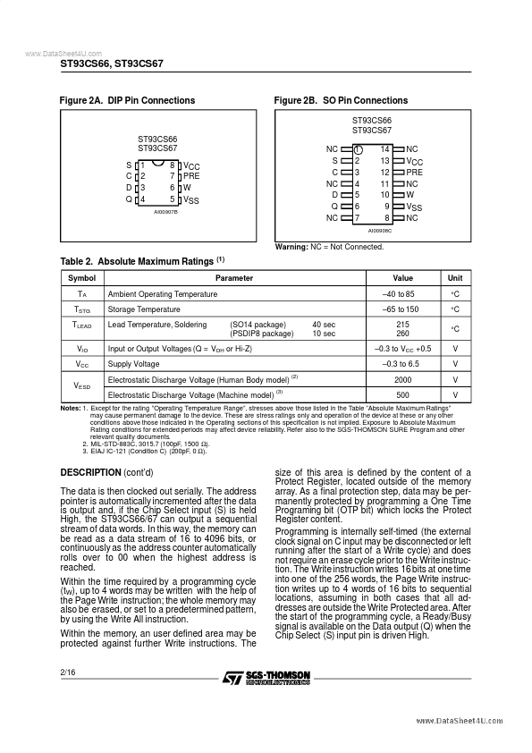
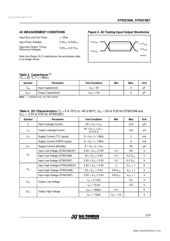
The ST93CS66 and ST93CS67 are 4K bit Electrically Erasable Programmable Memory (EEPROM) fabricated with SGS-THOMSON’s High Endurance Single Polysilicon CMOS technology. A Read instruction loads the address of the first word to be read into an internal address pointer. Table 1. Signal Names S D Q C PRE W VCC VSS Chip Select Input Serial Data Input Serial Data Output Serial Clock Protect Enable Write Enable Supply Voltage Ground VCC D C S PRE W ST93CS66 ST93CS67 Q VSS AI00906B June 1997 This is information on a product still in production bu t not recommended for new de signs. 1/16 ST93CS66, ST93CS67 Figure 2A. DIP Pin Connections Figure 2B. SO Pin Connections ST93CS66 ST93CS67 ST93CS66 ST93CS67 S C D Q 1 2 3 4 8 7 6 5 AI00907B VCC PRE W VSS NC S C NC D Q NC 1 2 3 4 5 6 7 14 13 12 11 10 9 8 AI00908C NC VCC PRE NC W VSS NC Warning: NC = Not Connected. Table 2.ABSOLUTE MAXIMUM RATINGS
(1) Symbol TA TSTG TLEAD VIO VCC VESD Parameter Ambient Operating Temperature Storage Tempera...