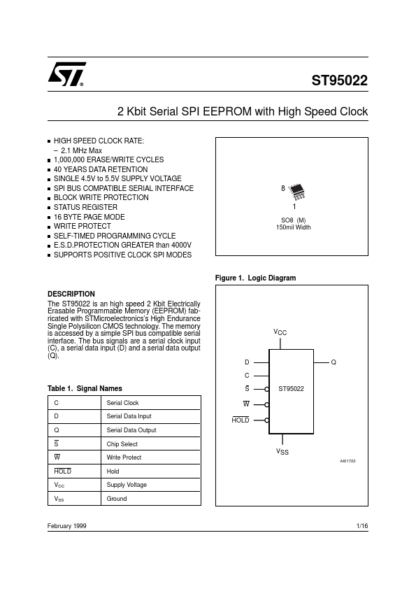
DESCRIPTION
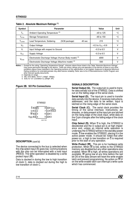
D C VCC Q Table 1. Signal Names C D Q S W HOLD VCC VSS Serial Clock Serial Data Input Serial Data Output Chip Select Write Protect Hold Supply Voltage Ground S W HOLD ST95022 VSS AI01722 February 1999 1/16 ST95022 Table 2. ABSOLUTE MAXIMUM RATINGS
(1) Symbol TA TSTG TLEAD VO VI VCC VESD Parameter Ambient Operating Temperature Storage Temperature Lead Temperature, Soldering Output Voltage Input Voltage with respect to Ground Supply Voltage Electrostatic Discharge Voltage (Human Body model) (3) Electrostatic Discharge Voltage (Machine model) (4) (2) Value –40 to 125 –65 to 150 Unit °C °C °C V V V V V (SO8 package) 40 sec 215 –0.3 to VCC +0.6 –0.3 to 6.5 –0.3 to 6.5 4000 500 Notes: 1. Except for the rating "Operating Temperature Range", stresses above those listed in the Table "ABSOLUTE MAXIMUM RATINGS
" may cause permanent damage to the device. These are stress ratings only and operation of the device at these or any other conditions above those indicated in the Operating sections of this specification is not implied. STMicroelectronics