DESCRIPTION
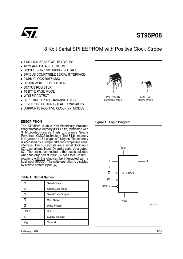
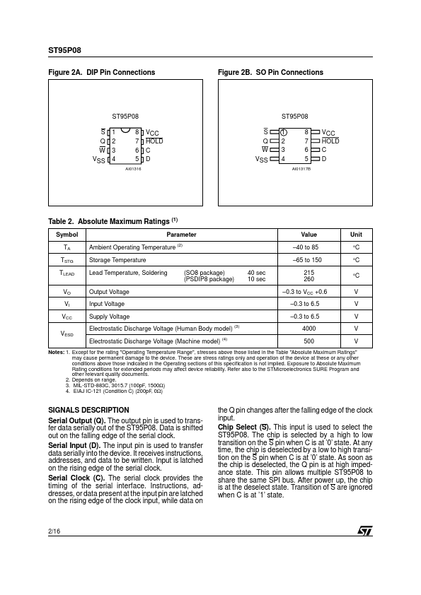
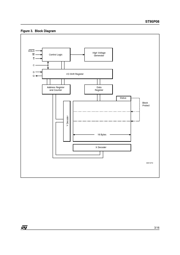
The bus signals are a serial clock input (C), a serial data input (D) and a serial data output (Q). The device connected to the bus is selected when the chip select input (S) goes low. Communications with the chip can be interrupted with a hold input (HOLD). The write operation is disabled by a write protect input (W). Figure 1. Logic Diagram VCC D C S ST95P08 Q Table 1. Signal Names C D Q S W HOLD VCC VSS February 1999 Serial Clock Serial Data Input Serial Data Output Chip Select Write Protect Hold Supply Voltage Ground W HOLD VSS AI01315 1/16 ST95P08 Figure 2A. DIP Pin Connections Figure 2B. SO Pin Connections ST95P08 S Q W VSS 1 2 3 4 8 7 6 5 AI01316 ST95P08 VCC HOLD C D S Q W VSS 1 2 3 4 8 7 6 5 AI01317B VCC HOLD C D Table 2. ABSOLUTE MAXIMUM RATINGS
(1) Symbol TA TSTG TLEAD VO VI VCC VESD Parameter Ambient Operating Temperature (2) Storage Temperature Lead Temperature, Soldering Output Voltage Input Voltage Supply Voltage Electrostatic Discharge Voltage (Human Body mod... STMicroelectronics