STMicroelectronics STB10NA40
N-CHANNEL POWER MOSFET
| Part No. | STB10NA40 |
|---|---|
| Datasheet | STB10NA40 Download |
| Manufacturer |  STMicroelectronics |
| Description | N-CHANNEL POWER MOSFET |
| Buy | Stock & Price |
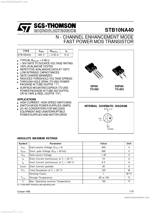
APPLICATIONS
n HIGH CURRENT, HIGH SPEED SWITCHING n SWITCH MODE POWER SUPPLIES (SMPS) n DC-AC CONVERTERS FOR WELDING EQUIPMENT AND UNINTERRUPTIBLE POWER SUPPLIES AND MOTOR DRIVE INTERNAL SCHEMATIC DIAGRAMABSOLUTE MAXIMUM RATINGS
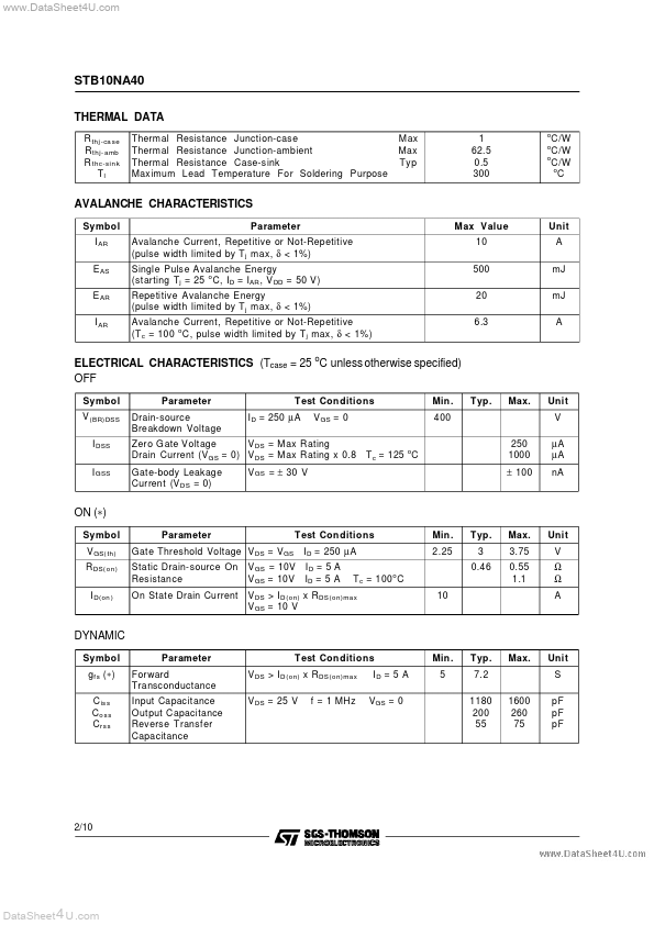
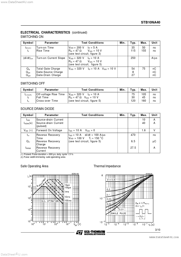
Symb ol V DS V DGR V GS ID ID I DM (● ) P tot T s tg Tj Parameter Drain-source Voltage (V GS = 0) Drain- gate Voltage (R GS = 20 k Ω ) Gate-source Voltage Drain Current (continuous) at T c = 25 C Drain Current (continuous) at T c = 100 o C Drain Current (pulsed) T otal Dissipation at T c = 25 C Derating Fact or Storage Temperature Max. O perating Junction Temperature o o Valu e 400 400 ± 30 10 6.3 40 125 1 -65 to 150 150 Unit V V V A A A W W/ oC o o C C (●) Pulse width limited by safe operating area October 1995 1/10 DataSheet 4 U .com STB10NA40 THERMAL DATA R thj -ca se R thj- amb R thc-sin k Tl Thermal Resistance Junction-case Thermal Resistance Junction-ambient Thermal Resistance Case-sink Maximum Lead T emperature For Soldering Purpose Max Max Typ 1 62.5...