STMicroelectronics STB20NK50Z
This device is an N-channel Zener-protected u Power MOSFET developed using d STMicroelectronics’ SuperMESH™ technology, ro achieved through optimization of ST’s well P established strip-based PowerMESH™ layout.| Part No. | STB20NK50Z |
|---|---|
| Datasheet | STB20NK50Z Download |
| Manufacturer |  STMicroelectronics |
| Description | N-CHANNEL POWER MOSFET |
| Buy | Stock & Price |

FEATURES
Type VDSS RDS(on) max ID PW STB20NK50Z 500 V < 0.27 Ω 17 A 190 W ct(s)● Extremely high dv/dt capability du
● 100% avalanche tested ro
● Gate charge minimized P
● Very low intrinsic capacitances te
● Very good manufacturing repeatability sole Application Ob
● Switching applications t(s) -
DESCRIPTION
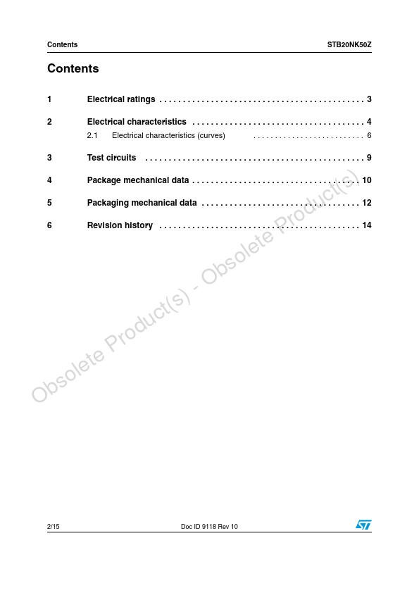
c In te addition to a significant reduction in on- resistance, this device is designed to ensure a le high level of dv/dt capability for the most Obso demanding applications. 3 1 D²PAK Figure 1. Internal schematic diagram D(2) G(1) S(3) AM01476v1 Table 1. Device summary Order code STB20NK50Z Marking B20NK50Z Package D²PAK Packaging Tape and reel March 2012 This is information on a discontinued product. Doc ID 9118 Rev 10 1/15 15 Contents Contents STB20NK50Z 1 Electrical ratings . . . . . . . . . . . . . . . . . . . . . . . . . . . . . . . . . . . . . . . . . . . . 3 2 Electrical characteristics . . . . . . . . . . . . . . . . . . . . . . . . . . . . . . . . . . . . . 4 2.1 Electrical characteristics (curves) ..........................