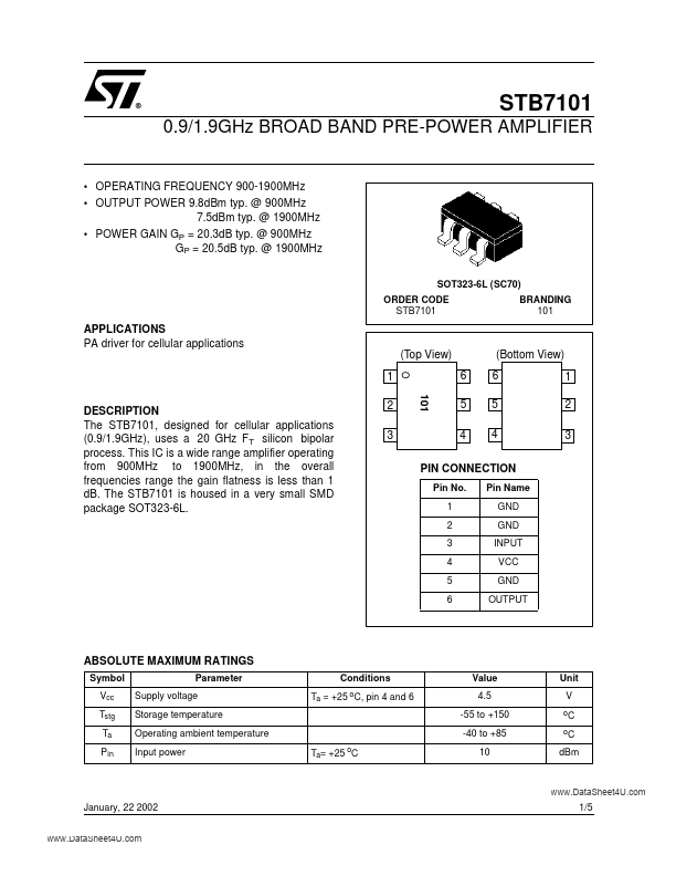
APPLICATIONS
PA driver for cellular applications (Top View) 1 101 DESCRIPTION
(Bottom View) 6 5 4 6 5 4 1 2 3 2 3 PIN CONNECTION Pin No. 1 2 3 4 5 6 Pin Name GND GND INPUT VCC GND OUTPUT ABSOLUTE MAXIMUM RATINGS
Symbol Vcc Tstg Ta Pin Parameter Supply voltage Storage temperature Operating ambient temperature Input power Ta= +25 oC Ta = Conditions +25 oC, pin 4 and 6 Value 4.5 -55 to +150 -40 to +85 10 Unit V o o C C dBm January, 22 2002 1/5 STB7101 ELECTRICAL CHARACTERISTICS
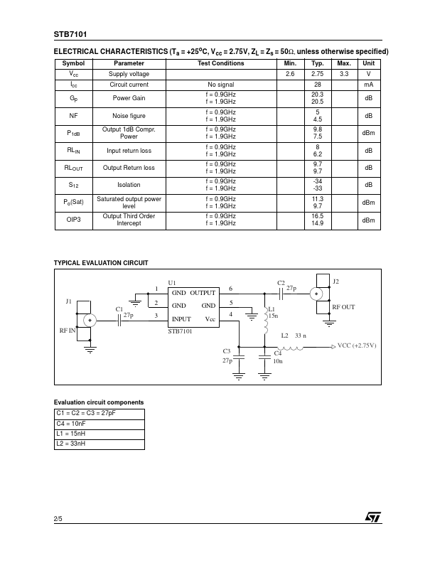
(Ta = +25oC, V cc = 2.75V, ZL = Zs = 50Ω, unless otherwise specified) Symbol Vcc Icc Gp NF P1dB RLIN RLOUT S12 Po(Sat) OIP3 Parameter Supply voltage Circuit current Power Gain Noise figure Output 1dB Compr. Power Input return loss Output Return loss Isolation Saturated output power level Output Third Order Intercept No signal f = 0.9GHz f = 1.9GHz f = 0.9GHz f = 1.9GHz f = 0.9GHz f = 1.9GHz f = 0.9GHz f = 1.9GHz f = 0.9GHz f = 1.9GHz f = 0.9GHz f = 1.9GHz f = 0.9GHz f = 1.9GHz f = 0.9GHz f = 1.9GHz Test Conditions Min. STMicroelectronics