STMicroelectronics STD15NF10
This MOSFET series realized with STMicroelectronics unique STripFET process has specifically been designed to minimize input capacitance and gate charge. It is therefore suitable as primary switch in advanced high-efficiency, high-frequency isolated DC-DC converters for Telecom and Computer applications.| Part No. | STD15NF10 |
|---|---|
| Datasheet | STD15NF10 Download |
| Manufacturer |  STMicroelectronics |
| Description | N-CHANNEL POWER MOSFET |
| Buy | Stock & Price |
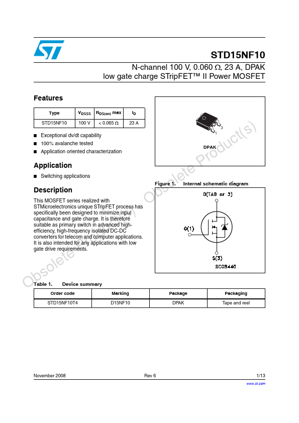
DESCRIPTION
It is also intended for any applications with low gate drive requirements.APPLICATIONS
s HIGH-EFFICIENCY DC-DC CONVERTERS s UPS AND MOTOR CONTROL DPAK TO-252 (Suffix ”T4”) INTERNAL SCHEMATIC DIAGRAMABSOLUTE MAXIMUM RATINGS
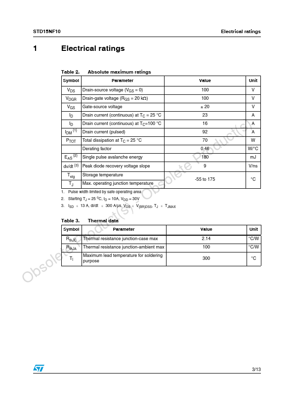
Symb ol V DS V DGR VGS ID ID I DM (● ) P tot dv/dt( 1 ) E AS ( 2 ) T st g Parameter Drain-source Voltage (VGS = 0) Drain- gate Voltage (R GS = 20 k Ω ) G ate-source Voltage Drain Current (continuous) at Tc = 25 oC Drain Current (continuous) at Tc = 100 o C Drain Current (pulsed) T otal Dissipation at Tc = 25 C Derating Factor Peak Diode Recovery voltage slope Single Pulse Avalanche Energy Storage Temperature o Value 100 100 ± 20 15 10 60 45 0.3 9 75 -65 to 175 175 Unit V V V A A A W W /o C V/ns mJ o o C C 1/6 Max. Operating Junction Temperature Tj (●) Pulse width limited by safe operating area ( 2) starting Tj = 25 oC, ID =24A , VDD = 50V April 2000 (1) I SD ≤ 80 A, di/dt ≤ 300A/µs, VDD ≤ V(BR)DSS, Tj ≤ TJMA STD15NF10 THERMAL DATA R thj -case R thj -am...