STMicroelectronics STD17NF25
This Power MOSFET has been developed using STMicroelectronics' unique STripFET process, which is specifically designed to minimize input capacitance and AM01475v1_noZen gate charge. This renders the device suitable for use as primary switch in advanced high-efficiency isolated DC-DC converters for telecom and computer applications, and applications with low gate charge driving requirements.| Part No. | STD17NF25 |
|---|---|
| Datasheet | STD17NF25 Download |
| Manufacturer |  STMicroelectronics |
| Description | N-channel Power MOSFET |
| Buy | Stock & Price |

FEATURES
TAB 23 1 DPAK D(2, TAB) Order code VDS RDS(on) max. ID STD17NF25 250 V 165 mΩ 17 A● Exceptional dv/dt capability
● 100% avalanche tested
● Low gate charge
APPLICATIONS
● Switching applications G(1)DESCRIPTION
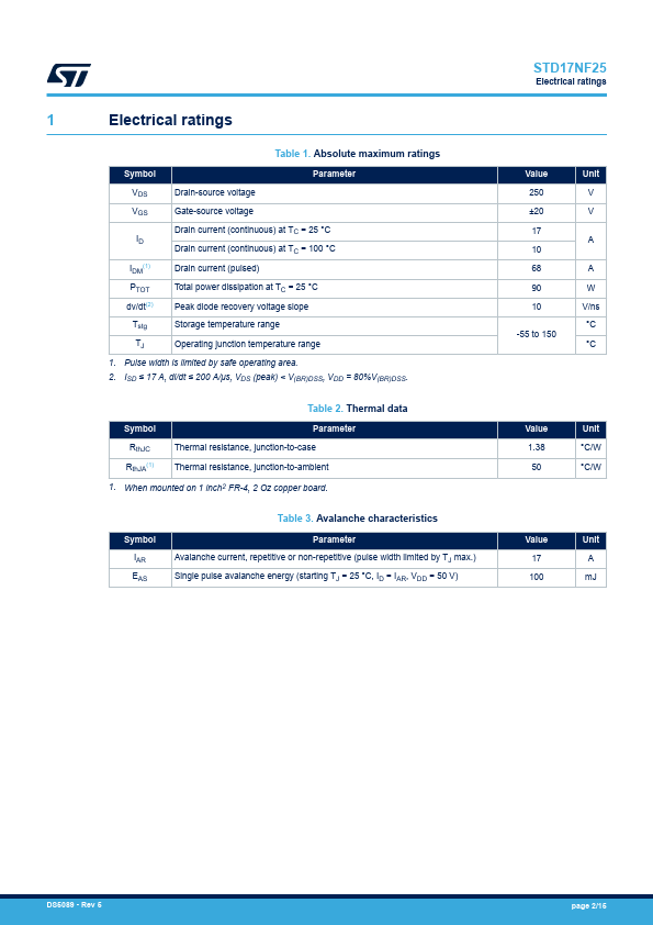
S(3) Product status link STD17NF25 Product summary Order code STD17NF25 Marking 17NF25 Package DPAK Packing Tape and reel DS5089 - Rev 5 - August 2023 For further information contact your local STMicroelectronics sales office. STD17NF25 Electrical ratings 1 Electrical ratings Table 1. Absolute maximum ratings Symbol Parameter VDS Drain-source voltage VGS Gate-source voltage Drain current (continuous) at TC = 25 °C ID Drain current (continuous) at TC = 100 °C IDM(1) Drain current (pulsed) PTOT Total power dissipation at TC = 25 °C dv/dt(2) Peak diode recovery voltage slope Tstg Storage temperature range TJ Operating junction temperature range 1. Pulse width is limited by safe operating area. 2. ISD ≤ 17 A, di/dt ≤ 200 A/μs, VDS (peak) < V(BR)DSS, VDD = 80%V(BR)DSS. Table 2.