STMicroelectronics STD20N06
This series of POWER MOSFETS represents the latest development in low voltage technology. The ultra high cell density process (UHD) produced with fine geometries on advanced equipment gives the device extremely low RDS(on) as well as good switching performance and high avalanche energy capability.| Part No. | STD20N06 |
|---|---|
| Datasheet | STD20N06 Download |
| Manufacturer |  STMicroelectronics |
| Description | N-CHANNEL MOSFET |
| Buy | Stock & Price |
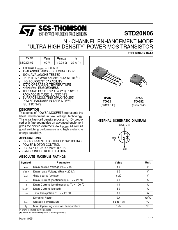
DESCRIPTION
APPLICATIONS
HIGH CURRENT, HIGH SPEED SWITCHING s POWER MOTOR CONTROL s DC-DC & DC-AC CONVERTERS s SYNCRONOUS RECTIFICATION s INTERNAL SCHEMATIC DIAGRAMABSOLUTE MAXIMUM RATINGS
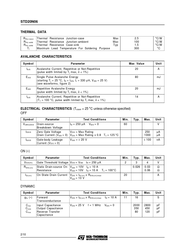
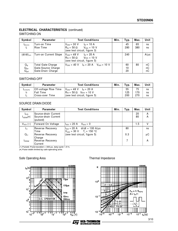
Symbol VD S V DG R V GS ID ID ID M(●) P tot T stg Tj Parameter Drain-source Voltage (V GS = 0) Drain- gate Voltage (R GS = 20 kΩ ) Gate-source Voltage Drain Current (continuous) at T c = 25 oC Drain Current (continuous) at T c = 100 C Drain Current (pulsed) Total Dissipation at Tc = 25 C Derating Factor Storage Temperature Max. Operating Junction Temperature o o Value 60 60 ± 20 20 14 80 60 0.4 -65 to 175 175 Unit V V V A A A W W/o C o o C C (*) Current limited by the package (●) Pulse width limited by safe operating area (*) March 1995 1/10 STD20N06 THERMAL DATA R thj-cas e Rthj- amb Rthj- amb Tl Thermal Resistance Junction-case Thermal Resistance Junction-ambient Thermal Resistance Case-sink Maximum Lead Temperature For Soldering Purpose Max Max Typ 2.5 100 1.5 300 o o C/W C/W o C/W o C AVALANCHE...