STMicroelectronics STD3PS25-1
The new patented STrip layout coupled with the Company’s proprietary edge termination structure, makes it suitable in coverters for lighting applications.| Part No. | STD3PS25-1 |
|---|---|
| Datasheet | STD3PS25-1 Download |
| Manufacturer |  STMicroelectronics |
| Description | P-CHANNEL MOSFET |
| Buy | Stock & Price |
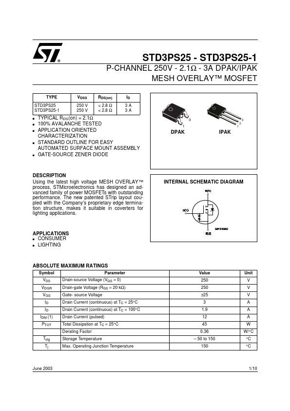
DESCRIPTION
Using the latest high voltage MESH OVERLAY™ process, STMicroelectronics has designed an advanced family of power MOSFETs with outstanding performance. INTERNAL SCHEMATIC DIAGRAMAPPLICATIONS
s CONSUMER s LIGHTINGABSOLUTE MAXIMUM RATINGS
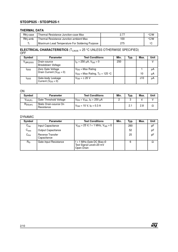
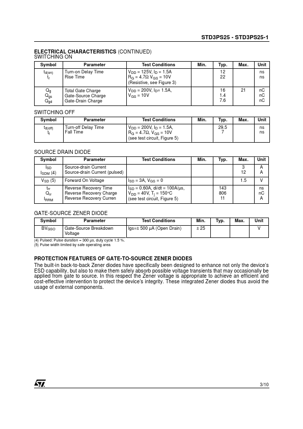
Symbol Parameter VDS Drain-source Voltage (VGS = 0) VDGR Drain-gate Voltage (RGS = 20 kΩ) VGS Gate- source Voltage ID Drain Current (continuous) at TC = 25°C ID Drain Current (continuous) at TC = 100°C IDM (1) Drain Current (pulsed) PTOT Total Dissipation at TC = 25°C Derating Factor Tstg Storage Temperature Tj Max. Operating Junction Temperature Value 250 250 ±25 3 1.9 12 45 0.36 – 50 to 150 150 Unit V V V A A A W W/°C °C °C June 2003 1/10 STD3PS25 - STD3PS25-1 THERMAL DATA Rthj-case Thermal Resistance Junction-case Max Rthj-amb Thermal Resistance Junction-ambient Max Tl Maximum Lead Temperature For Soldering Purpose 2.77 100 275 °C/W °C/W °CELECTRICAL CHARACTERISTICS
(TCASE = 25 °C UNLESS OTHERWISE SPECIFIED) OFF Symbol Parameter Test Conditions Min.