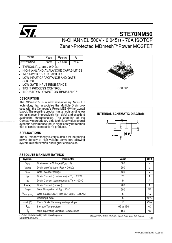
DESCRIPTION
The adoption of the Company’s proprietary strip technique yields overall dynamic performance that is significantly better than that of similar competition’s products. APPLICATIONS
The MDmesh™ family is very suitable for increasing power density of high voltage converters allowing system miniaturization and higher efficiencies. INTERNAL SCHEMATIC DIAGRAM ABSOLUTE MAXIMUM RATINGS
Symbol VDS VDGR VGS ID ID IDM (l) PTOT VESD(G-S) dv/dt (1) Tstg Tj Parameter Drain-source Voltage (VGS = 0) Drain-gate Voltage (RGS = 20 kΩ) Gate- source Voltage Drain Current (continuous) at TC = 25°C Drain Current (continuous) at TC = 100°C Drain Current (pulsed) Total Dissipation at TC = 25°C Gate source ESD(HBM-C=100pF, R=15KΩ) Derating Factor Peak Diode Recovery voltage slope Storage Temperature Max. Operating Junction Temperature Value 500 500 ±30 70 44 280 600 6 5 15 –65 to 150 150 (1)ISD ≤60A, di/dt ≤400A/µs, V DD ≤ V(BR)DSS, Tj ≤ T JMAX Unit V V V A A A W KV W/°C V/ns °C °C 1/8 (●)Pulse widt... STMicroelectronics