STI24NM65N
STI24NM65N is N-channel Power MOSFET manufactured by STMicroelectronics.
STW24NM65N-STI24NM65N-STF24NM65N STB24NM65N
- STP24NM65N
N-channel 650 V
- 0.16 Ω
- 19 A
- TO-220
- TO-220FP
- D2PAK I2PAK
- TO-247 second generation MDmesh™ Power MOSFET
Features
.. Type
VDSS (@TJmax) 710 V 710 V 710 V 710 V 710 V
RDS(on) max < 0.19 Ω < 0.19 Ω < 0.19 Ω < 0.19 Ω < 0.19 Ω
STB24NM65N STI24NM65N STF24NM65N STP24NM65N STW24NM65N
19 A 19 A 19 A(1) 19 A 19 A
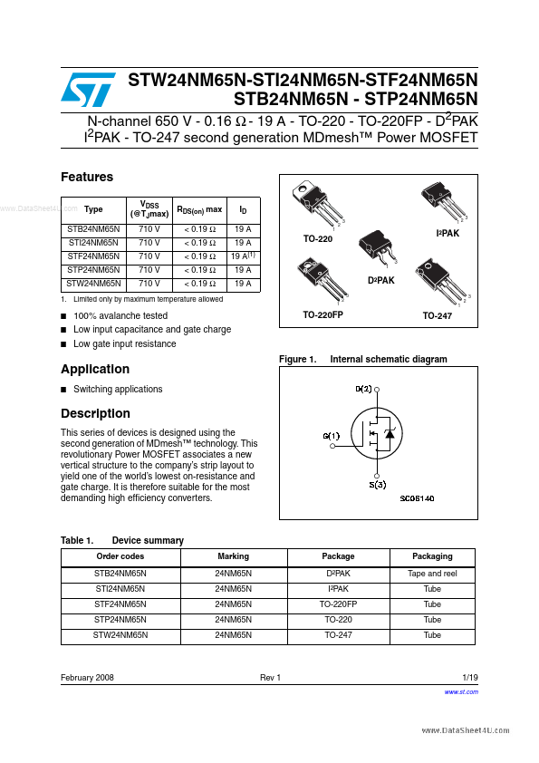
3 12
TO-220
3 1
I²PAK
D²PAK
3 1 2
1. Limited only by maximum temperature allowed
- -
- 2 1
100% avalanche tested Low input capacitance and gate charge Low gate input resistance
TO-220FP
TO-247
Figure 1.
Internal schematic diagram
Application...