STMicroelectronics STN2NE06
This Power Mosfet is the latest development of STMicroelectronics unique ”Single Feature Size™” stip-based process. The resulting transistor shows extremely high packing density for low on-resistance, rugged avalanche characteristics and less critical alignment steps therefore a remarkable manufacturing reproducibility.| Part No. | STN2NE06 |
|---|---|
| Datasheet | STN2NE06 Download |
| Manufacturer |  STMicroelectronics |
| Description | N-CHANNEL POWER MOSFET |
| Buy | Stock & Price |
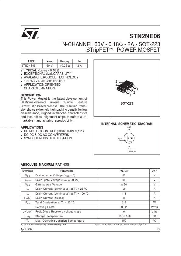
DESCRIPTION
1 SOT-223 2 INTERNAL SCHEMATIC DIAGRAMAPPLICATIONS
s DC MOTOR CONTROL (DISK DRIVES,etc.) s DC-DC & DC-AC CONVERTERS s SYNCHRONOUS RECTIFICATIONABSOLUTE MAXIMUM RATINGS
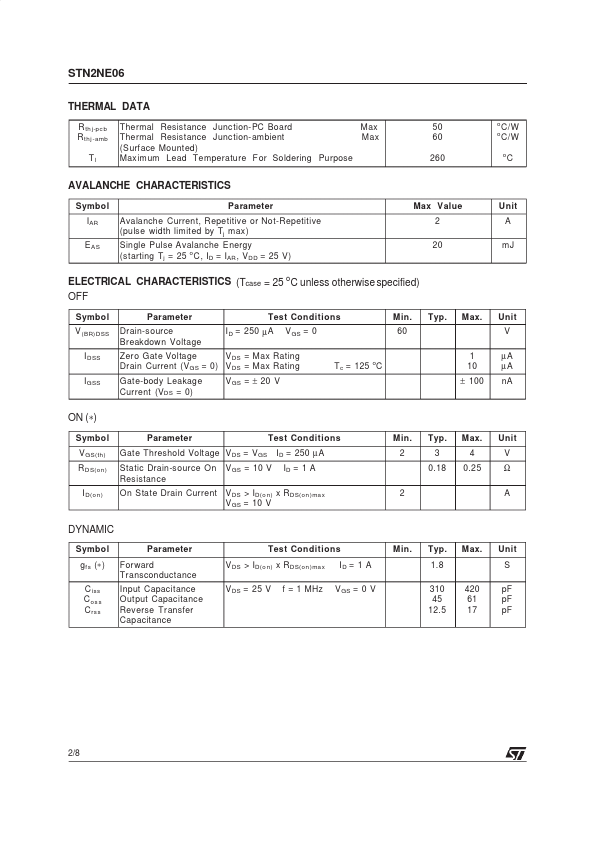
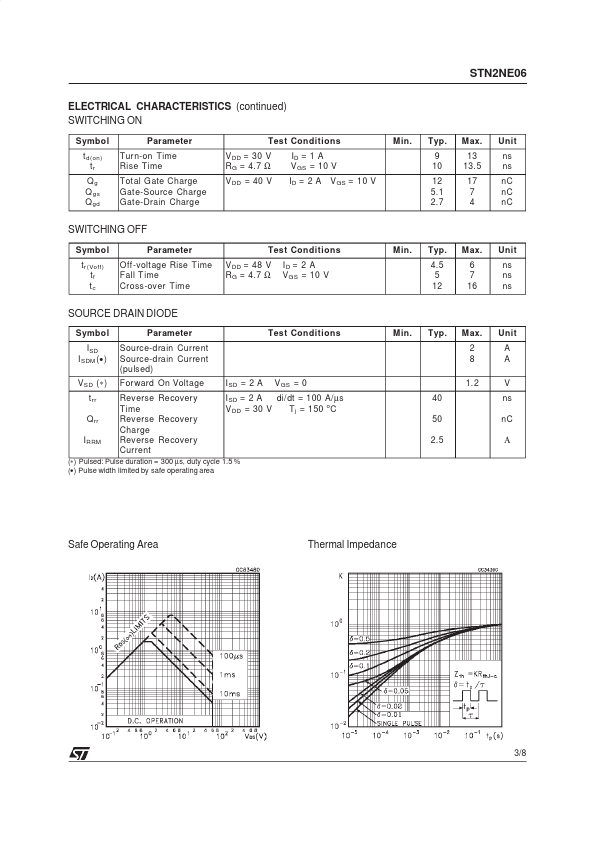
Symb ol V DS V DGR VGS ID ID I DM (● ) P tot dv/dt( 1 ) T st g Tj April 1999 Parameter Drain-source Voltage (VGS = 0) Drain- gate Voltage (R GS = 20 k Ω ) Gate-source Voltage Drain Current (continuous) at Tc = 25 C Drain Current (continuous) at Tc = 100 C Drain Current (pulsed) Total Dissipation at T c = 25 oC Derating F actor Peak Diode Recovery voltage slope Storage T emperature Max. Operating Junction Temperature o o Value 60 60 ± 20 2 1.3 8 2.5 0.02 6 -65 to 150 150 ( 1) ISD ≤ 8 A, di/dt ≤ 200 A/µs, VDD ≤ V(BR)DSS, Tj ≤ TJMAX Unit V V V A A A W W /o C V/ns o o C C 1/8 (●) Pulse width limited by safe operating area STN2NE06 THERMAL DATA R th j-pc b R thj -amb Tl Thermal Resistance Junction-PC Board Max Thermal Resistance Junction-ambient Max (Surf ace Mounted) Maximum Lead Temperature F or Soldering Pur...