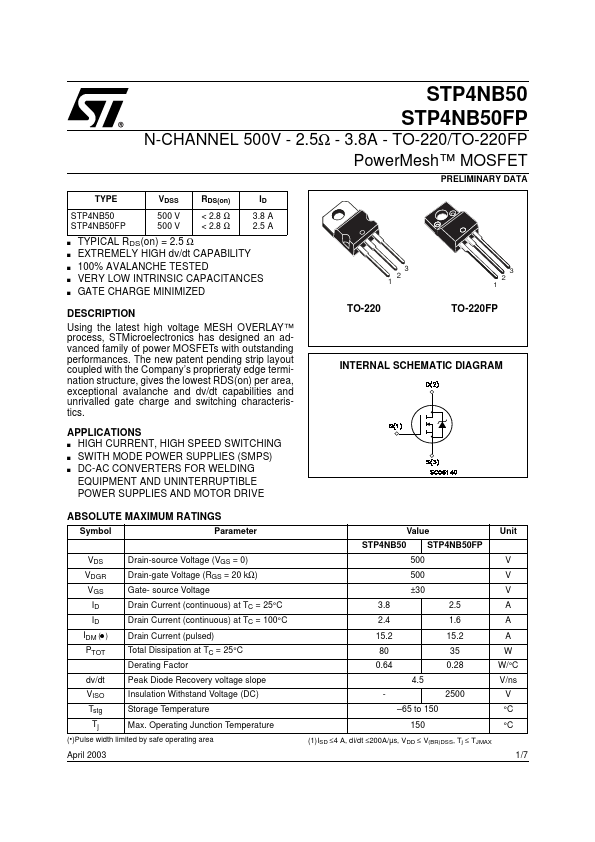
DESCRIPTION
Using the latest high voltage MESH OVERLAY™ process, STMicroelectronics has designed an advanced family of power MOSFETs with outstanding performances. APPLICATIONS
HIGH CURRENT, HIGH SPEED SWITCHING s SWITH MODE POWER SUPPLIES (SMPS) s DC-AC CONVERTERS FOR WELDING EQUIPMENT AND UNINTERRUPTIBLE POWER SUPPLIES AND MOTOR DRIVE s TO-220FP INTERNAL SCHEMATIC DIAGRAM ABSOLUTE MAXIMUM RATINGS
Symbol VDS VDGR VGS ID ID IDM ( ) PTOT dv/dt VISO Tstg Tj Parameter STP4NB50 Drain-source Voltage (VGS = 0) Drain-gate Voltage (RGS = 20 kΩ) Gate- source Voltage Drain Current (continuous) at TC = 25°C Drain Current (continuous) at TC = 100°C Drain Current (pulsed) Total Dissipation at TC = 25°C Derating Factor Peak Diode Recovery voltage slope Insulation Withstand Voltage (DC) Storage Temperature Max. Operating Junction Temperature –65 to 150 150 (1)ISD ≤4 A, di/dt ≤200A/µs, VDD ≤ V(BR)DSS, Tj ≤ TJMAX Value STP4NB50FP 500 500 ±30 3.8 2.4 15.2 80 0.64 4.5 2500 2.5 1.6 15.2 35 0.28 Unit V V V... STMicroelectronics