STW23NM60N Description
This series of devices is designed using the second generation of MDmesh™ technology. This revolutionary Power MOSFET associates a new vertical structure to the pany’s strip layout to yield one of the world’s lowest on-resistance and gate charge. It is therefore suitable for the most demanding high efficiency converters.
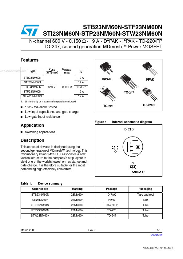
STW23NM60N Key Features
- 19 A 19 A 650 V 0.180 Ω 19 A (1)
- Switching