DESCRIPTION
Main features are: minimum working supply voltage of 3V, low quiescent current, low cnumber of external components, good ripple rejecution, no cross-over distortion, low power dissipadtion. roOutput power: Po = 2W at 12V/8Ω, 1.6W at 9V/4Ω Pand 1.2W at 9V/8Ω. leteABSOLUTE MAXIMUM RATINGS
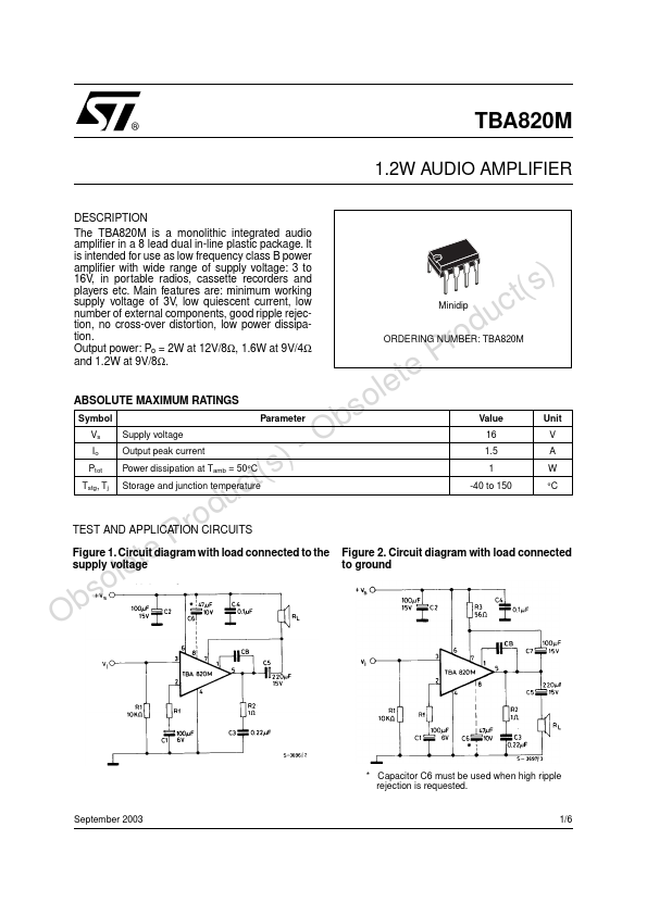
soSymbol Parameter bVs - OIo )Ptot t(sTstg, Tj Supply voltage Output peak current Power dissipation at Tamb = 50°C Storage and junction temperature Minidip ORDERING NUMBER: TBA820M Value 16 1.5 1 -40 to 150 Unit V A W °C roducTEST AND APPLICATION CIRCUITS PFigure 1. Circuit diagram with load connected to the Figure 2. Circuit diagram with load connected Obsoletesupply voltage STMicroelectronics