DESCRIPTION
ABSOLUTE MAXIMUM RATINGS
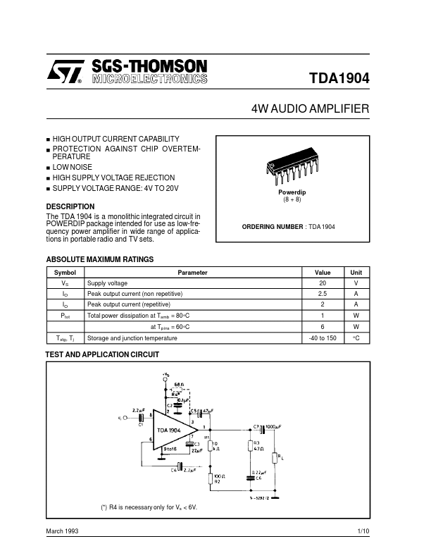
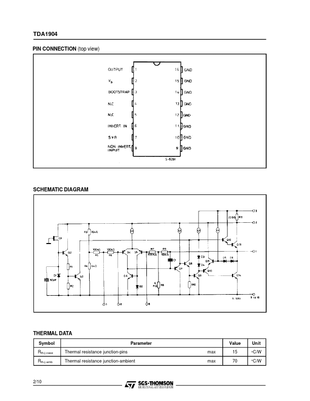
Symbol VS IO IO Ptot Supply voltage Peak output current (non repetitive) Peak output current (repetitive) Total power dissipation at Tamb = 80°C at Tpins = 60°C Tstg, Tj Storage and junction temperature Parameter Value 20 2.5 2 1 6 -40 to 150 Unit V A A W W °C Powerdip (8 + 8) ORDERING NUMBER : TDA 1904 TEST AND APPLICATION CIRCUIT (*) R4 is necessary only for Vs < 6V. March 1993 1/10 TDA1904 PIN CONNECTION (top view) SCHEMATIC DIAGRAM THERMAL DATA Symbol Rth-j-case Rth-j-amb Thermal resistance junction-pins Thermal resistance junction-ambient Parameter max max Value 15 70 Unit °C/W °C/W 2/10 TDA1904 ELECTRICAL CHARACTERISTICS
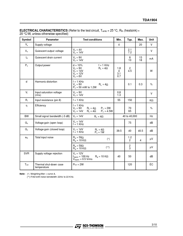
(Refer to the test circuit, Tamb = 25 °C, Rth (heatsink) = 20 °C/W, unless otherwisw specified) Symbol Vs Vo Id Po Parameter Supply voltage Quiescent output voltage Quiescent drain current Output power Vs = 4V Vs = 14V Vs = 9V Vs = 14V d = 10% Vs = 9V Vs = 14V Vs = 12V Vs = 6V f = 1 KHz RL = 4Ω 1.8 4 3.1 0.7 Test conditions Min. STMicroelectronics