DESCRIPTION
The device provides a high output current capability (up to 3.5A) very low harmonic and cross-over distortion. Completely safe operation is guaranteed due to protection against DC and AC short circuit between all pins and ground, thermal over-range, load dump voltage surge up to 40V and fortuitous open ground. ABSOLUTE MAXIMUM RATINGS
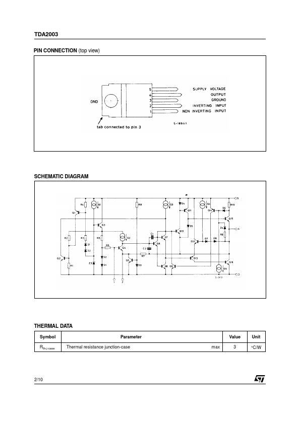
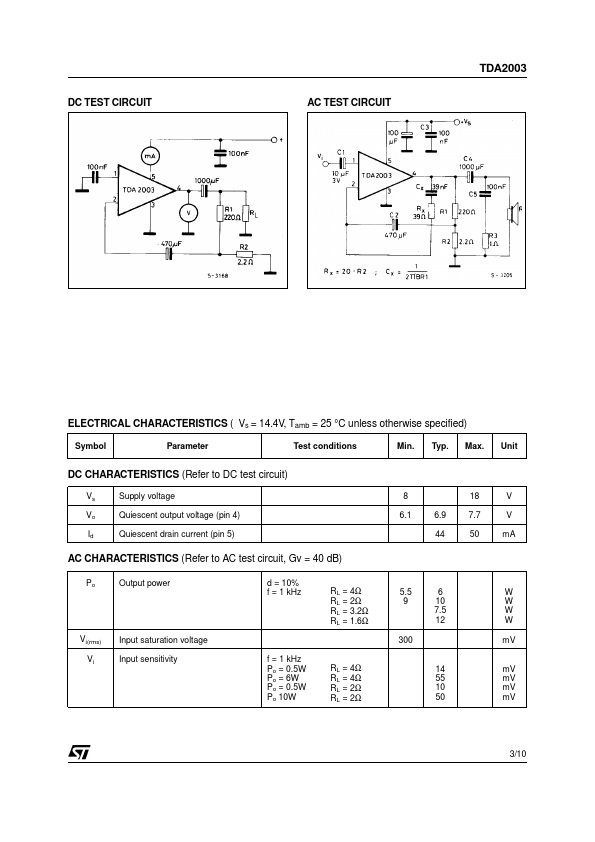
Symbol VS VS VS IO IO Ptot Tstg, Tj Parameter Peak supply voltage (50ms) DC supply voltage Operating supply voltage Output peak current (repetitive) Output peak current (non repetitive) Power dissipation at Tcase = 90°C Storage and junction temeperature TEST CIRCUIT PENTAWATT ORDERING NUMBERS : TDA 2003H TDA 2003V Value 40 28 18 3.5 4.5 20 -40 to 150 Unit V V V A A W °C September 2013 1/10 TDA2003 PIN CONNECTION (top view) SCHEMATIC DIAGRAM THERMAL DATA Symbol Parameter Rth-j-case Thermal resistance junction-case 2/10 Value max 3 Unit °C/W DC TEST CIRCUIT AC TEST CIRCUIT TDA2003 ELECTRICAL CHARACTERISTICS
( Vs = 14.4V, Tamb = 25 °C unless otherwise specified) Symbol Parameter Test conditions Min. STMicroelectronics