DESCRIPTION
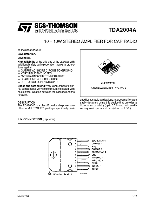
PIN CONNECTION (top view) March 1995 1/10 TDA2004A ABSOLUTE MAXIMUM RATINGS
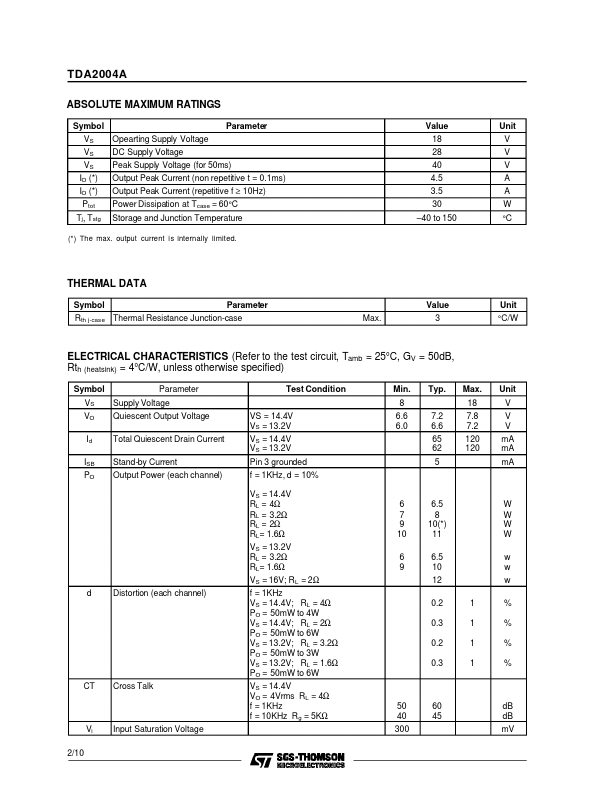
Symbol VS VS VS IO (*) IO (*) Ptot Tj, Tstg Opearting Supply Voltage DC Supply Voltage Peak Supply Voltage (for 50ms) Output Peak Current (non repetitive t = 0.1ms) Output Peak Current (repetitive f ≥ 10Hz) Power Dissipation at Tcase = 60°C Storage and Junction Temperature Parameter Value 18 28 40 4.5 3.5 30 –40 to 150 Unit V V V A A W °C (*) The max. output current is internally limited. THERMAL DATA Symbol Parameter Max. Value 3 Unit °C/W Rth j-case Thermal Resistance Junction-case ELECTRICAL CHARACTERISTICS
(Refer to the test circuit, Tamb = 25°C, GV = 50dB, Rth (heatsink) = 4°C/W, unless otherwise specified) Symbol VS VO Id ISB PO Parameter Supply Voltage Quiescent Output Voltage Total Quiescent Drain Current Stand-by Current Output Power (each channel) VS = 14.4V VS = 13.2V VS = 14.4V VS = 13.2V Pin 3 grounded f = 1KHz, d = 10% VS = 14.4V RL = 4Ω RL = 3.2Ω RL = 2Ω RL= 1.6Ω VS = 13.2V RL = 3.2Ω... STMicroelectronics