DESCRIPTION
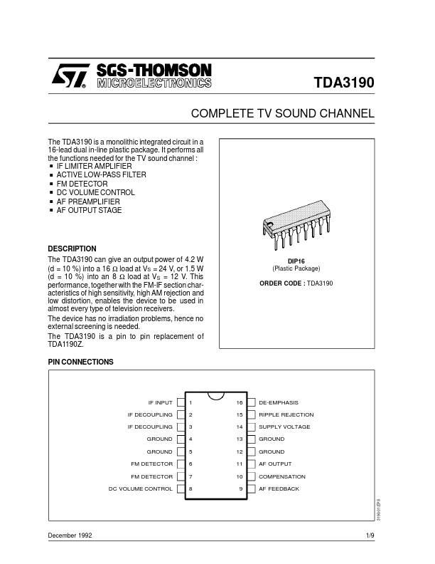
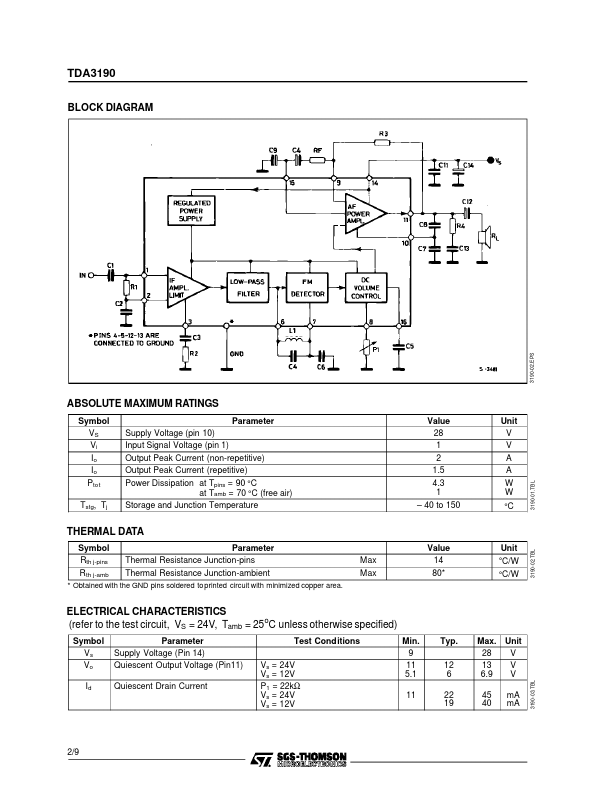
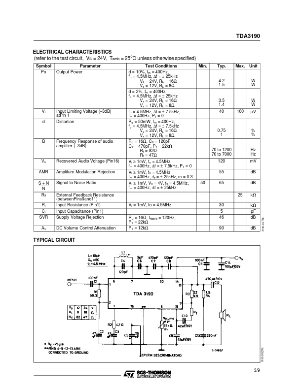
The TDA3190 can give an output power of 4.2 W (d = 10 %) into a 16 Ω load at VS = 24 V, or 1.5 W (d = 10 %) into an 8 Ω load at VS = 12 V. The device has no irradiation problems, hence no external screening is needed. The TDA3190 is a pin to pin replacement of TDA1190Z. PIN CONNECTIONS DIP16 (Plastic Package) ORDER CODE : TDA3190 IF INPUT IF DECOUPLING IF DECOUPLING GROUND GROUND FM DETECTOR FM DETECTOR DC VOLUME CONTROL 1 2 3 4 5 6 7 8 16 15 14 13 12 11 10 9 DE-EMPHASIS RIPPLE REJECTION SUPPLY VOLTAGE GROUND GROUND AF OUTPUT COMPENSATION AF FEEDBACK 3190-01.EPS December 1992 1/9 TDA3190 BLOCK DIAGRAM ABSOLUTE MAXIMUM RATINGS
Symbol VS Vi Io Io Ptot Tstg, Tj Parameter Supply Voltage (pin 10) Input Signal Voltage (pin 1) Output Peak Current (non-repetitive) Output Peak Current (repetitive) Power Dissipation at Tpins = 90 °C at Tamb = 70 °C (free air) Storage and Junction Temperature Value 28 1 2 1.5 4.3 1 – 40 to 150 Unit V V A A W W °C THERMAL DATA Symbol Rth j-pins R th j-... STMicroelectronics