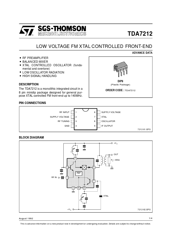
DESCRIPTION
PIN CONNECTIONS RF INPUT SUPPLY VOLTAGE RF TUNING GND 1 2 3 4 8 7 6 5 SUP PLY VOLTAGE XTAL OSC ILLATOR IF OUTPUT 7 212-01.EPS BLOCK DIAGRAM +V S OUT 3 RL = 300Ω 2 REF RF IN 1 5 7 4 8 6 XTAL +V S 7 212-02.EPS August 1992 1/4 This is advance info rmation on a new product now in development or undergoing evaluation. Details are subject to change without notice. TDA7212 ABSOLUTE MAXIMUM RATINGS
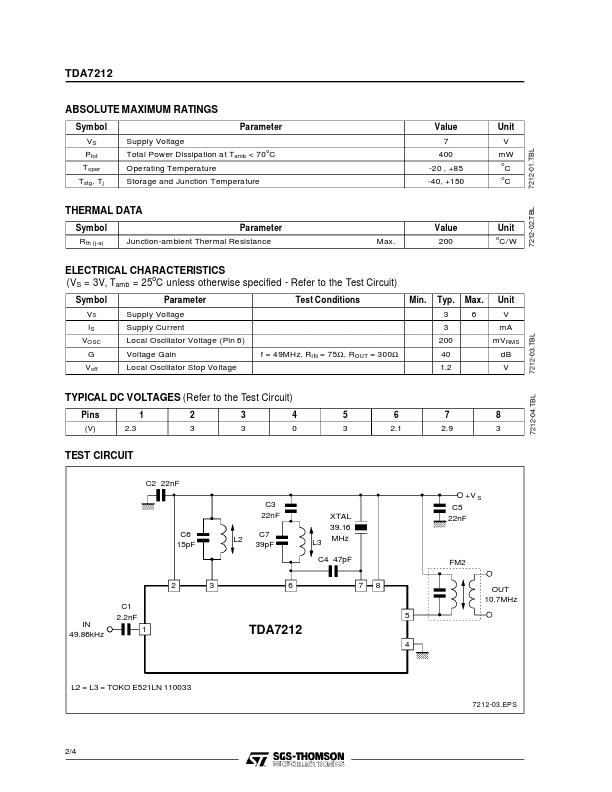
Symbol VS P tot T oper T stg , Tj Supply Voltage Total Power Dissipation a t Tamb < 70oC Operating Tem pera ture Storage and Junction Temperature Parameter Value 7 400 -20 , +85 -40, +150 Unit V mW o o C C Symbol R th (j-a) Parameter Junction-am bient Thermal Resistance Max. Value 200 Unit o C/ W ELECTRICAL CHARACTERISTICS
o (VS = 3V, Tamb = 25 C unless otherwise specified - Refer to the Test Circuit) Symbol VS IS VOSC G V off Parameter Supply Voltage Supply Current Local Oscillator Voltage (Pin 6) Voltage Gain Local Oscillator Stop Voltage Test Conditions Min. Typ. 3 3 200 Max. 6 Unit V... STMicroelectronics