DESCRIPTION
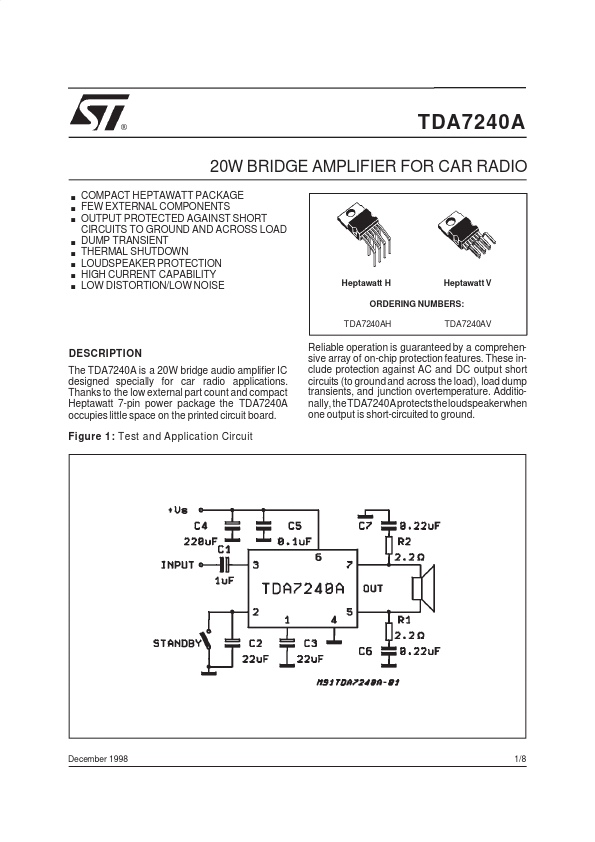
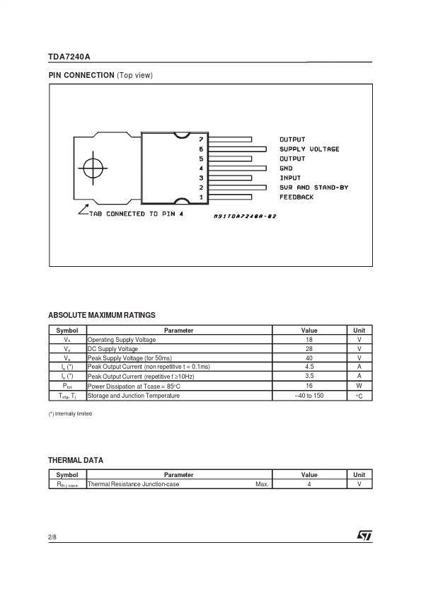
Figure 1: Test and Application Circuit Reliable operation is guaranteed by a comprehensive array of on-chip protection features. Additionally, theTDA7240Aprotectstheloudspeakerwhen one output is short-circuited to ground. December 1998 1/8 TDA7240A PIN CONNECTION (Top view) ABSOLUTE MAXIMUM RATINGS
Symbol Vs Vs Vs Io (*) Io (*) Ptot Tstg, Tj Operating Supply Voltage DC Supply Voltage Peak Supply Voltage (for 50ms) Peak Output Current (non repetitive t = 0.1ms) Peak Output Current (repetitive f ≥10Hz) Power Dissipation at Tcase = 85°C Storage and Junction Temperature Parameter Value 18 28 40 4.5 3.5 16 –40 to 150 Unit V V V A A W °C (*) Internally limited THERMAL DATA Symbol Rth j-case Parameter Thermal Resistance Junction-case Max. Value 4 Unit V 2/8 TDA7240A ELECTRICAL CHARACTERISTICS
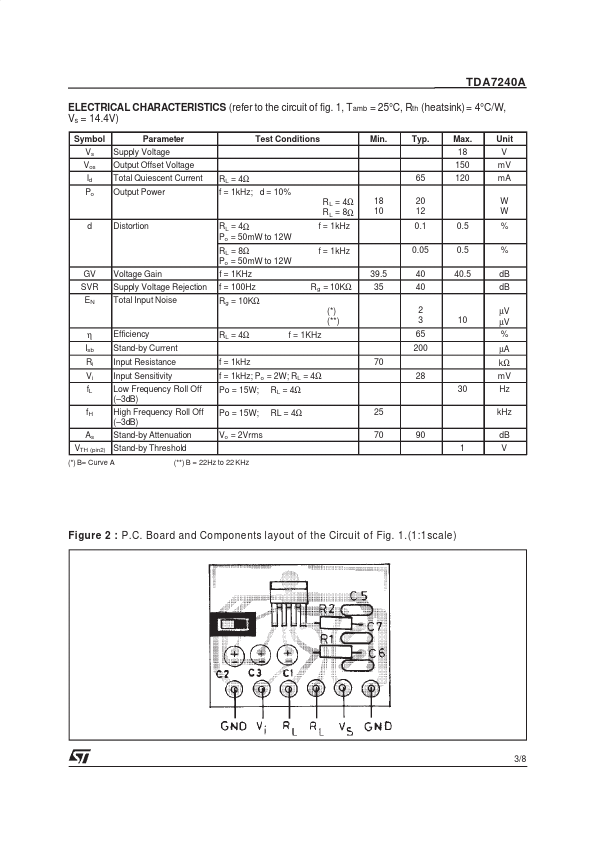
(refer to the circuit of fig. 1, T amb = 25°C, Rth (heatsink) = 4°C/W, Vs = 14.4V) Symbol Vs Vos Id Po Parameter Supply Voltage Output Offset Voltage Total Quiescent Current Output Power RL =... STMicroelectronics