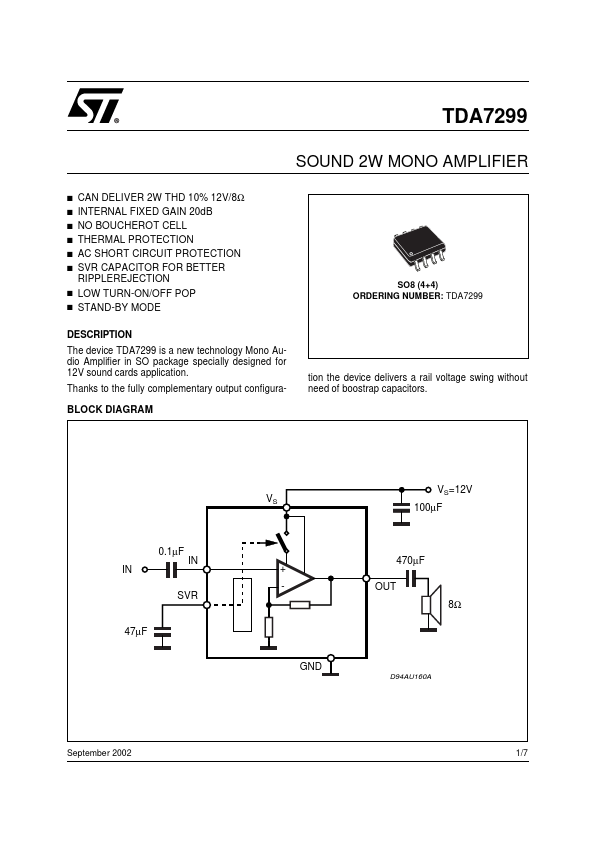
DESCRIPTION
The device Thanks to the fully complementary output configuraBLOCK DIAGRAM tion the device delivers a rail voltage swing without need of boostrap capacitors. VS VS=12V 100µF 0.1µF IN IN + OUT 470µF SVR 47µF 8Ω GND D94AU160A September 2002 1/7 TDA7299 ABSOLUTE MAXIMUM RATINGS
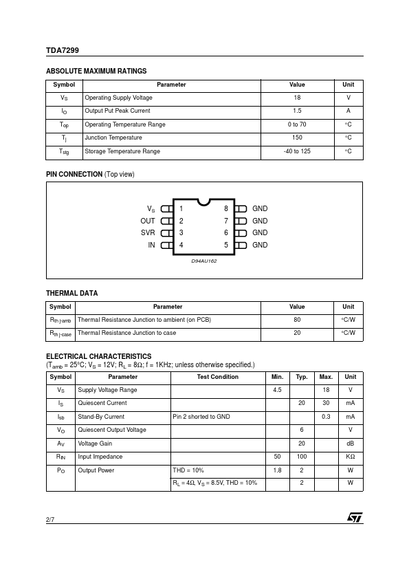
Symbol VS IO Top Tj Tstg Operating Supply Voltage Output Put Peak Current Operating Temperature Range Junction Temperature Storage Temperature Range Parameter Value 18 1.5 0 to 70 150 -40 to 125 Unit V A °C °C °C PIN CONNECTION (Top view) VS OUT SVR IN 1 2 3 4 D94AU162 8 7 6 5 GND GND GND GND THERMAL DATA Symbol Rth j-amb Rth j-case Parameter Thermal Resistance Junction to ambient (on PCB) Thermal Resistance Junction to case Value 80 20 Unit °C/W °C/W ELECTRICAL CHARACTERISTICS
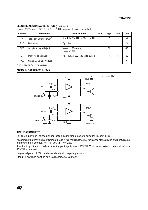
(Tamb = 25°C; VS = 12V; RL = 8Ω; f = 1KHz; unless otherwise specified.) Symbol VS IS Isb VO AV RIN PO Parameter Supply Voltage Range Quiescent Current Stand-By Current Quiescent Output Voltage Voltage Gain Input Impedance Output Power THD = 10% RL = 4Ω, VS = 8.5V, THD = 10% 50 1.8 Pin 2 shorted to GND 6 20 100 2 2 Test Condition Min. STMicroelectronics