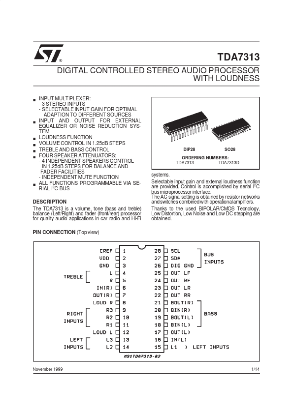
DESCRIPTION
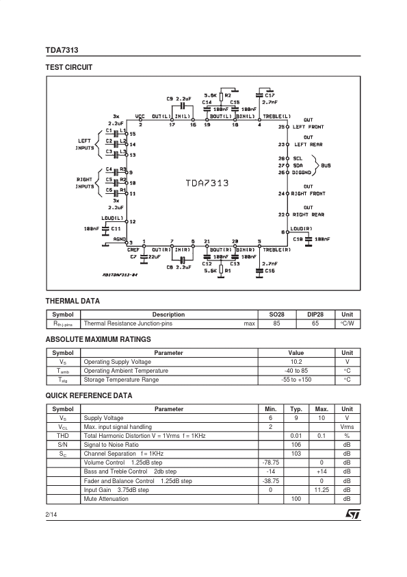
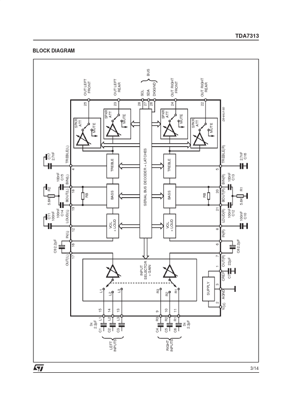
Selectable input gain and external loudness function are provided. Control is accomplished by serial I2C bus microprocessor interface. Thanks to the used BIPOLAR/CMOS Tecnology, Low Distortion, Low Noise and Low DC stepping are obtained. November 1999 1/14 TDA7313 TEST CIRCUIT THERMAL DATA Symbol R th j-pins DESCRIPTION
Thermal Resistance Junction-pins max SO28 85 DIP28 65 Unit °C/W ABSOLUTE MAXIMUM RATINGS
Symbol VS T amb Tstg Operating Supply Voltage Operating Ambient Temperature Storage Temperature Range Parameter Value 10.2 -40 to 85 -55 to +150 Unit V °C °C QUICK REFERENCE DATA Symbol VS VCL THD S/N SC Supply Voltage Max. input signal handling Total Harmonic Distortion V = 1Vrms f = 1KHz Signal to Noise Ratio Channel Separation f = 1KHz Volume Control 1.25dB step 2db step 1.25dB step -78.75 -14 -38.75 0 100 Bass and Treble Control Input Gain 3.75dB step Parameter Min. 6 2 0.01 106 103 0 +14 0 11.25 0.1 Typ. 9 Max. 10 Unit V Vrms % dB dB dB dB dB dB dB Fader and Balance... STMicroelectronics