ABSOLUTE MAXIMUM RATINGS
Symbol V4, V9 I8, I5, I1 I22, I15 Ptot Tstg, Tj V14 Supply Voltage Vs Video Out, QSSout, AF AM Out, DC Output Current Pin 22 and Pin 15 Input Current Total Power Dissipation (Tamb = 70 °C) Storage and Junction Temperature Voltage at Pin 14 Parameter Value 15 10 1 2 – 40 to 150 Vs Unit V mA mA °C 8120B-01.TBL 8120B-02.TBL W THERMAL DATA Symbol R th j–amb Thermal Resistance Parameter Max Value 40 Unit °C/W 2/6 8120B-02.EPS TDA8120B ELECTRICAL CHARACTERISTICS
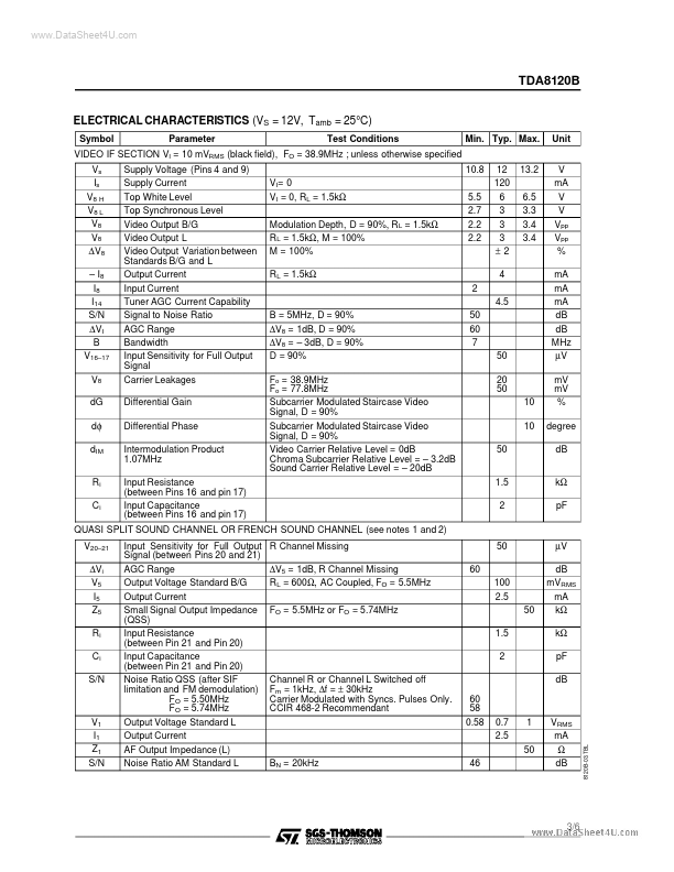
(VS = 12V, Tamb = 25°C) Symbol Vs Is V8 H V8 L V8 V8 ∆ V8 – I8 I8 I14 S/N ∆ VI B V16–17 V8 dG dφ dIM Ri Ci Parameter Supply Voltage (Pins 4 and 9) Supply Current Top White Level Top Synchronous Level Video Output B/G Video Output L Video Output Variation between Standards B/G and L Output Current Input Current Tuner AGC Current Capability Signal to Noise Ratio AGC Range Bandwidth Input Sensitivity for Full Output Signal Carrier Leakages Differential Gain Differential Phase Intermodulation Product 1.07MHz Inpu... STMicroelectronics