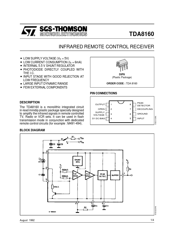
DESCRIPTION
BLOCK DIAGRAM PEAK DETECTOR DECOUPLING GROUND INPUT 8160-01.EPS OUTPUT OPEN SUPPLY VOLTAGE D1 DC BIAS 1 2 3 4 8 7 6 5 August 1992 1/4 8160-02.EPS TDA8160 ABSOLUTE MAXIMUM RATINGS
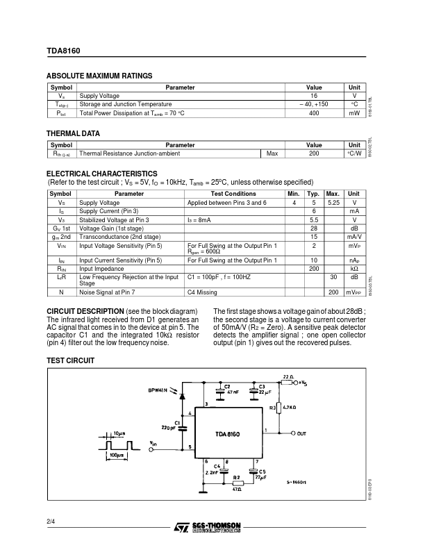
8160-01.TBL 8160-03.EPS 8160-03.TBL 8160-02.TBL Symbol Vs Tstg–j Ptot Parameter Supply Voltage Storage and Junction Temperature Total Power Dissipation at Tamb = 70 °C Value 16 – 40, +150 400 Unit V °C mW THERMAL DATA Symbol R th (j-a) Parameter Thermal Resistance Junction-ambient Max Value 200 Unit °C/W ELECTRICAL CHARACTERISTICS
(Refer to the test circuit ; VS = 5V, fO = 10kHz, Tamb = 25oC, unless otherwise specified) Symbol VS IS V3 GV 1st gm 2nd VIN IIN R IN LfR N Parameter Supply Voltage Supply Current (Pin 3) Stabilized Voltage at Pin 3 Voltage Gain (1st stage) Transconductance (2nd stage) Input Voltage Sensitivity (Pin 5) Input Current Sensitivity (Pin 5) Input Impedance Low Frequency Rejection at the Input Stage Noise Signal at Pin 7 Test Conditions Applied between Pins 3 and 6 I3 = 8mA Min. STMicroelectronics