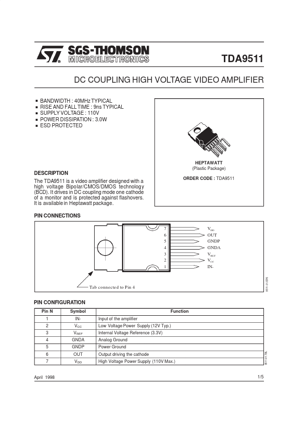
DESCRIPTION
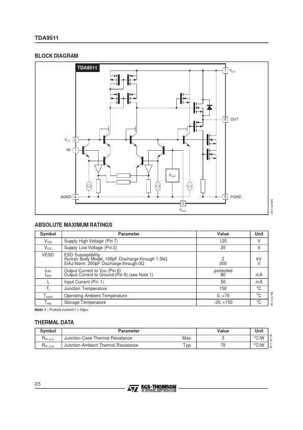
It is available in Heptawatt package. PIN CONNECTIONS 7 6 5 4 3 2 1 VDD OUT GNDP GNDA VRE F VCC IN9511-01.EPS ORDER CODE : TDA9511 Tab co nnecte d to Pin 4 PIN CONFIGURATION Pin N 1 2 3 4 5 6 7 Symbol INVCC VREF GNDA GNDP OUT VDD Input of the amplifier Low Voltage Power Supply (12V Typ.) Internal Voltage Reference (3.3V) Analog Ground Power Ground Output driving the cathode High Voltage Power Supply (110V Max.) 9511-01.TBL Function April 1998 1/5 TDA9511 BLOCK DIAGRAM TDA9511 7 VDD 6 OUT VCC 2 IN- 1 VREF AGND 4 3 VREF 5 PGND 9511-02.EPS ABSOLUTE MAXIMUM RATINGS
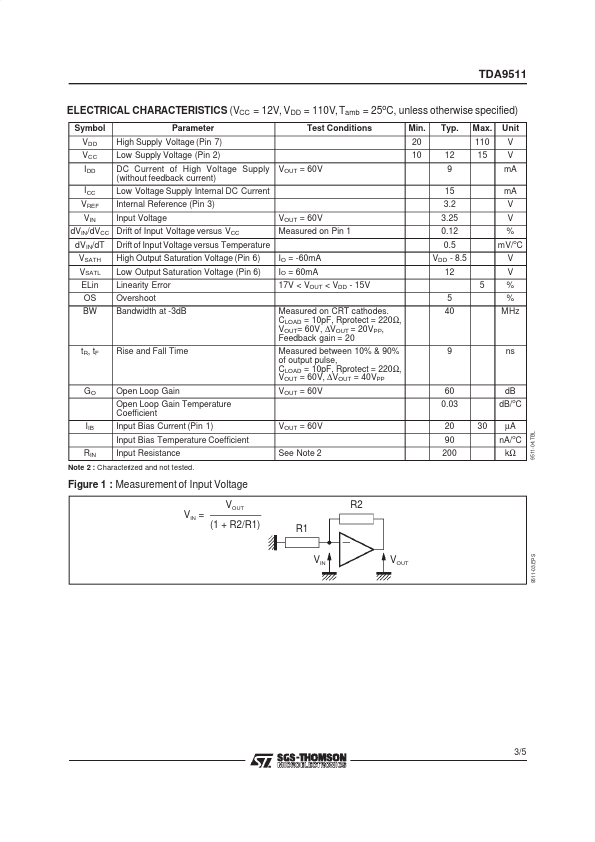
Symbol V DD V CC VESD Supply High Voltage (Pin 7) Supply Low Voltage (Pin 2) ESD Susceptibility Human Body Model, 100pF Discharge through 1.5kΩ EIAJ Norm, 200pF Discharge through 0Ω Output Current to VDD (Pin 6) Output Current to Ground (Pin 6) (see Note 1) Input Current (Pin 1) Junction Temperature Operating Ambient Temperature Storage Temperature Parameter Value 120 20 2 300 protected 80 50 150 0, +70 -20, +150 Uni... STMicroelectronics